

Rapid thermal process for silicon sheet capable of obtaining denuded zone and product thereof
A technology of rapid heat treatment and process method, applied in the direction of electrical components, semiconductor/solid-state device manufacturing, circuits, etc., can solve the problems that cannot reach 10μm, clean area thickness, etc.
- Summary
- Abstract
- Description
- Claims
- Application Information
AI Technical Summary
Problems solved by technology
Method used
Image

Examples
Embodiment
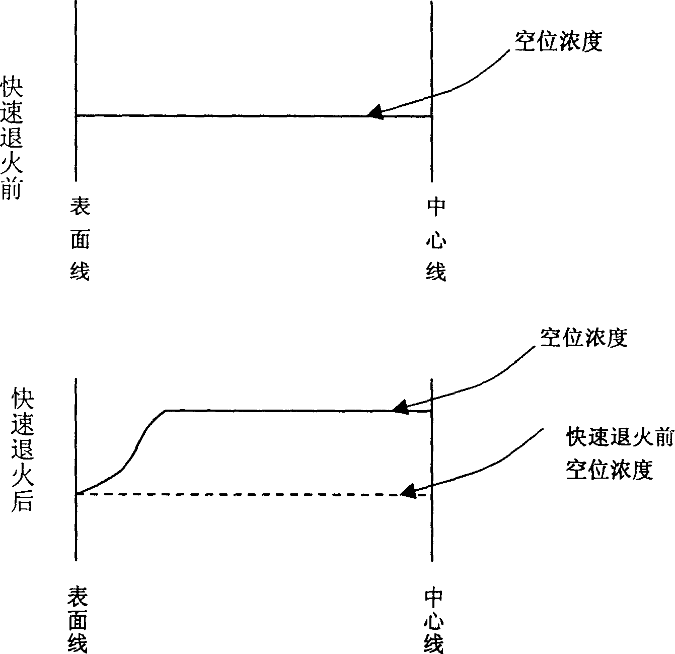
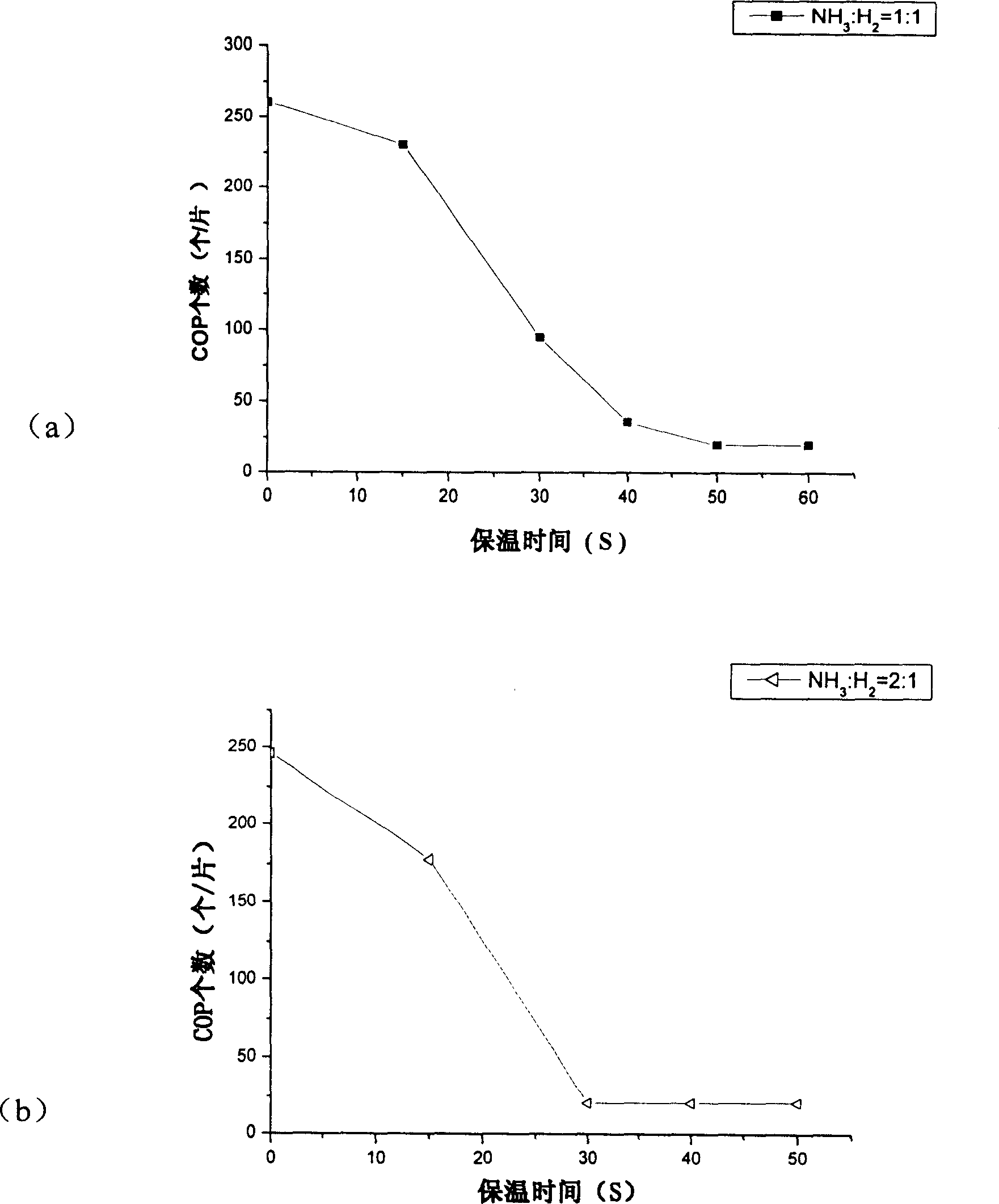
[0041] in H 2 / NH 3 / Ar atmosphere, using different cooling rates, the silicon wafers were subjected to RTA treatment process. During the experiment, except for the different holding time, other process conditions were the same. After RTA treatment, the density of COP was measured. The heat treatment process of 700°C for 4 hours and 900°C for 16 hours generates oxygen precipitation and obtains a clean area. The specific process parameters and experimental results are shown in Table 1.
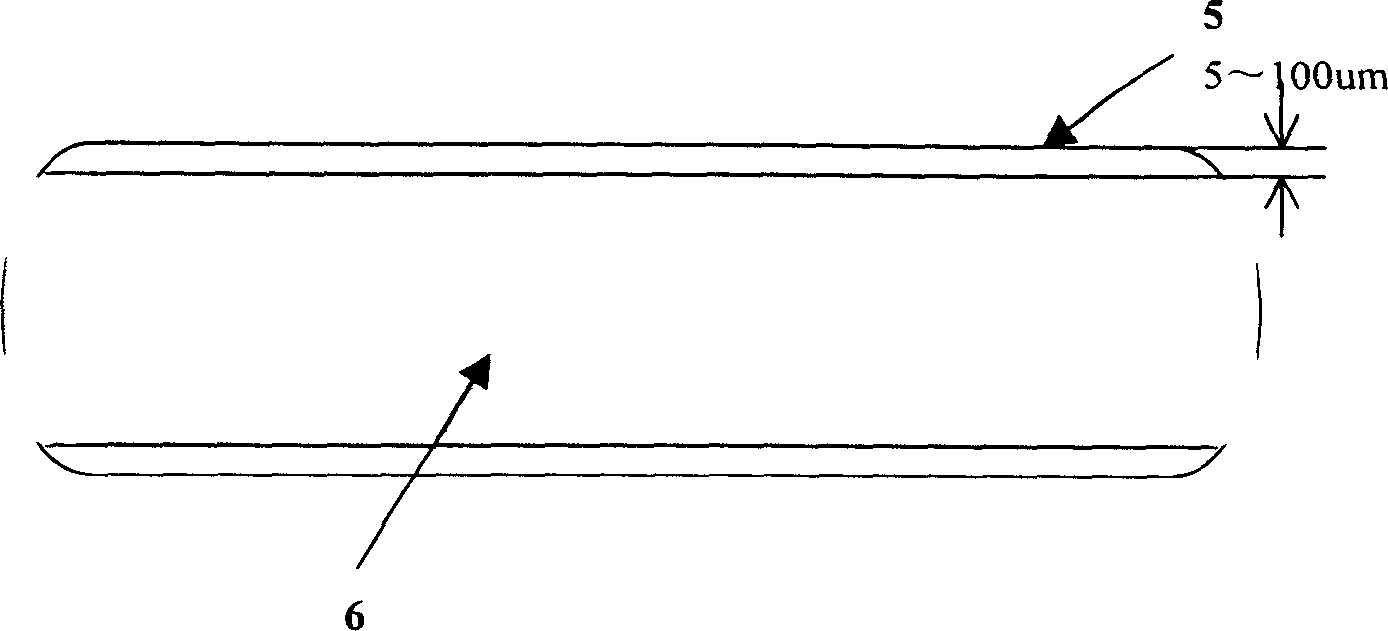
[0042] It can be seen from Table 1 that the thickness of the clean area becomes thinner as the holding time increases, and the oxygen precipitation density decreases as the holding time increases. The COP density decreases with the increase of holding time, but not all the time. 30s holding time is enough to eliminate COP, Figure 4 Clean area obtained for insulation 15S, such as Figure 4 as shown, Figure 4 The symbols in are represented as: the back side of the silicon wafer 1; the gett...
PUM
 Abstract
Description
Claims
Application Information