Process for fabricating semiconductor laser device

A technology of laser device and manufacturing method, which is applied in the direction of semiconductor laser device, semiconductor laser, structural details of semiconductor laser, etc., and can solve problems such as inability to reduce the interval of light-emitting points, inability to paste, large current resistance, etc.

Inactive Publication Date: 2006-09-27
PIONEER CORP
View PDF3 Cites 7 Cited by
  • Summary
  • Abstract
  • Description
  • Claims
  • Application Information

AI Technical Summary

Problems solved by technology

[0014] However, in this structure, a thick first substrate is provided between the first light-emitting element and the second light-emitting element. As described in the above-mentioned Patent Document 1, the first substrate (GaN substrate) usually has a thickness of about 100 μm. , so there is a problem that the distance between the light-emitting part (the position of the light-emitting point) of the first light-emitting element and the light-emitting part (the position of the light-emitting point) of the second light-emitting element is relatively large
[0019] In the semiconductor laser device of Patent Document 3, since the integration of two semiconductor lasers is carried out by directly pasting the first semiconductor light-emitting element and the second semiconductor light-emitting element, a semiconductor light-emitting element (e.g. In the case of a ridge-band semiconductor laser), the surfaces close to the light-emitting point cannot be pasted together, and the distance between the light-emitting points cannot be reduced.
In addition, in the semiconductor laser device of Patent Document 3, the GaAs contact layer is exposed by partially etching the AlGaInP system laser side including the GaAs substrate after bonding the two laser chips, but the state before etching The current confinement layer directly above the contact layer is also GaAs, so it is very difficult to stop the etch at the GaAs contact layer
In addition, in order to supply current from the bonding surface side, the current needs to flow through the contact layer from the in-plane direction, but since the contact layer is made of a semiconductor such as GaAs, there is a problem that the resistance in the current flow path is large.

Method used


Image

  • Process for fabricating semiconductor laser device
  • Process for fabricating semiconductor laser device
  • Process for fabricating semiconductor laser device

Examples


no. 1 approach

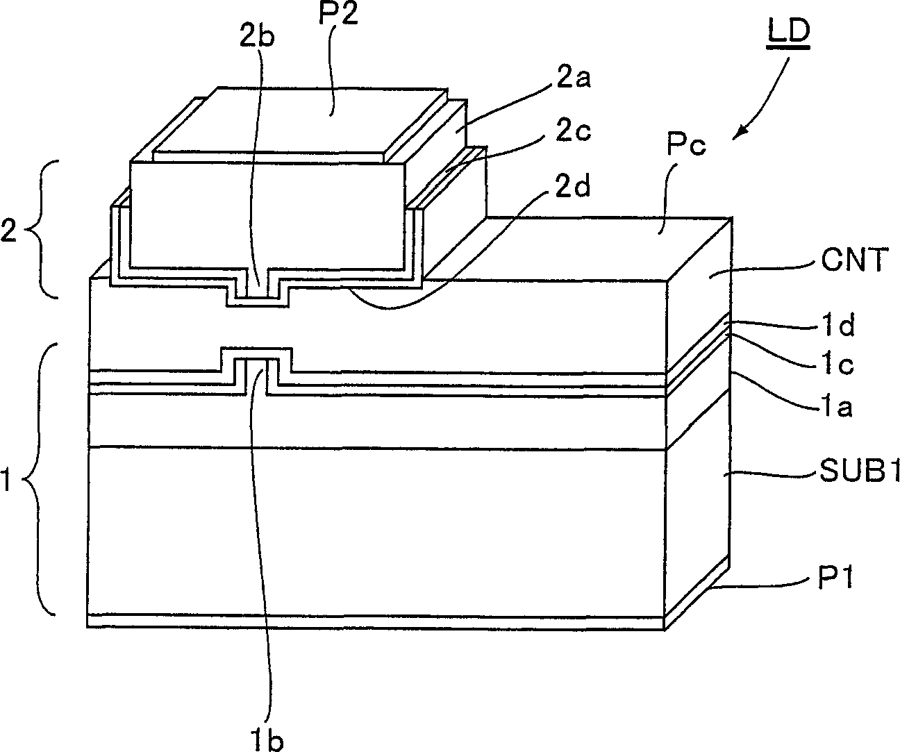
[0044] refer to figure 1 and figure 2 The first embodiment will be described. figure 1 is a perspective view showing an external structure of a semiconductor laser device manufactured by the manufacturing method of this embodiment, figure 2 It is a schematic diagram showing the manufacturing method of the semiconductor laser device of this embodiment.

[0045] exist figure 1 Among them, the semiconductor laser device LD manufactured according to this embodiment has a first light emitting element 1 and a second light emitting element 2 that emit laser light with different wavelengths, and the first and second light emitting elements are bonded by welding or the like of an adhesive layer CNT made of metal. The light emitting elements 1 and 2 are fixed and bonded as one.

[0046] The first light-emitting element 1 has: a semiconductor substrate SUB1 composed of a III-V compound semiconductor (for example, GaAs); on the semiconductor substrate SUB1, a first multilayer compos...

no. 2 Embodiment approach

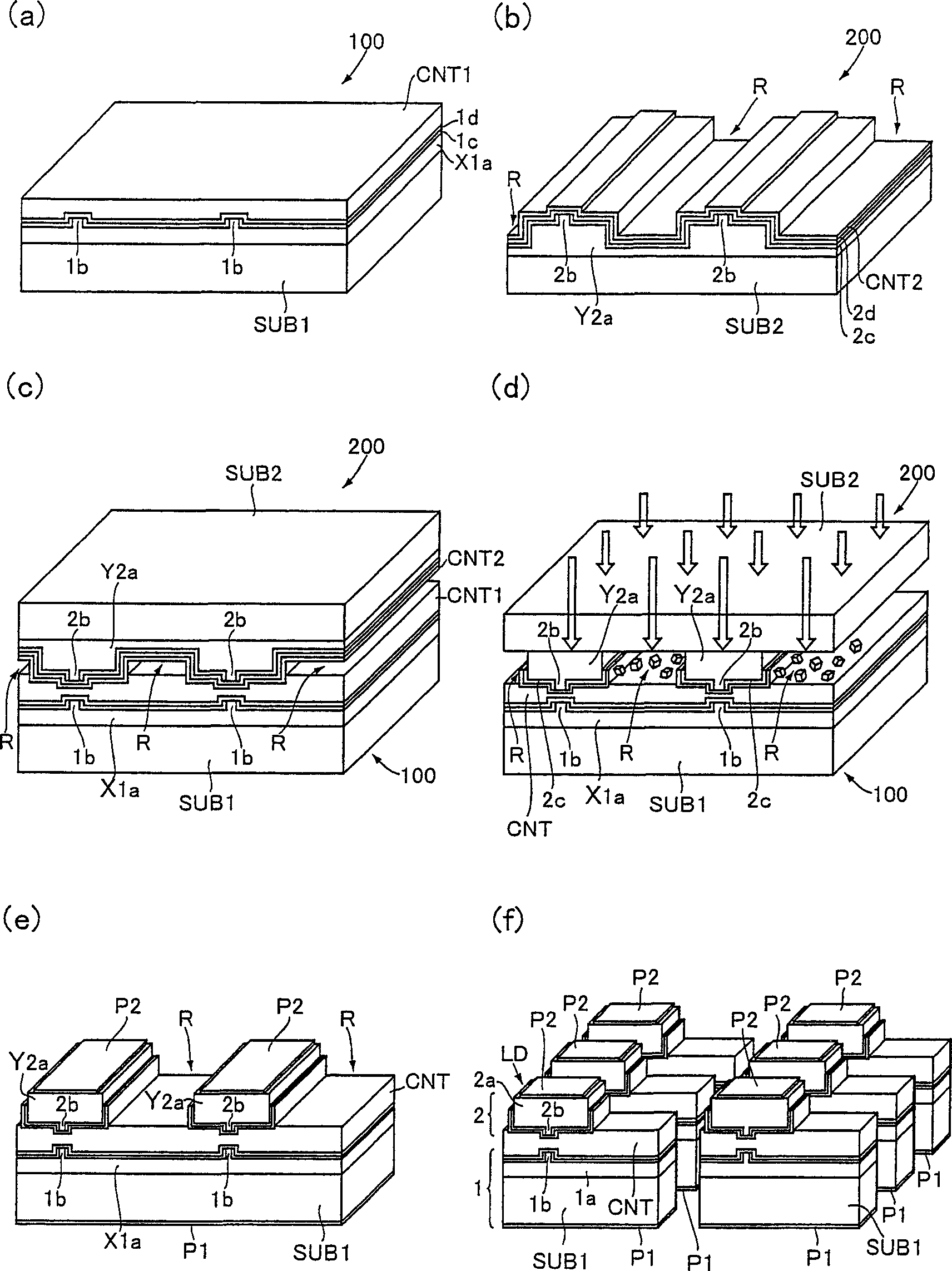
[0073] Below, refer to image 3 The second embodiment will be described. image 3 is a schematic diagram showing the manufacturing method of this embodiment, and the same symbols are used to denote and figure 2 same or equivalent parts.

[0074] The semiconductor laser device manufactured according to this embodiment basically has and figure 1 The semiconductor laser device shown has the same structure. However, as described below, the manufacturing method is different.

[0075] That is, to describe this production method, firstly, a image 3 The first intermediate product 100 and the second intermediate product 200 shown in (a) and (b). here, image 3 The 1st intermediate product 100 shown in (a) is made with figure 2 The intermediate product 100 shown in (a) has the same structure.

[0076] about image 3 The second intermediate product 200 shown in (b), and figure 2 The intermediate product 200 shown in (b) is different in that between the support substrate SUB...

Embodiment 1

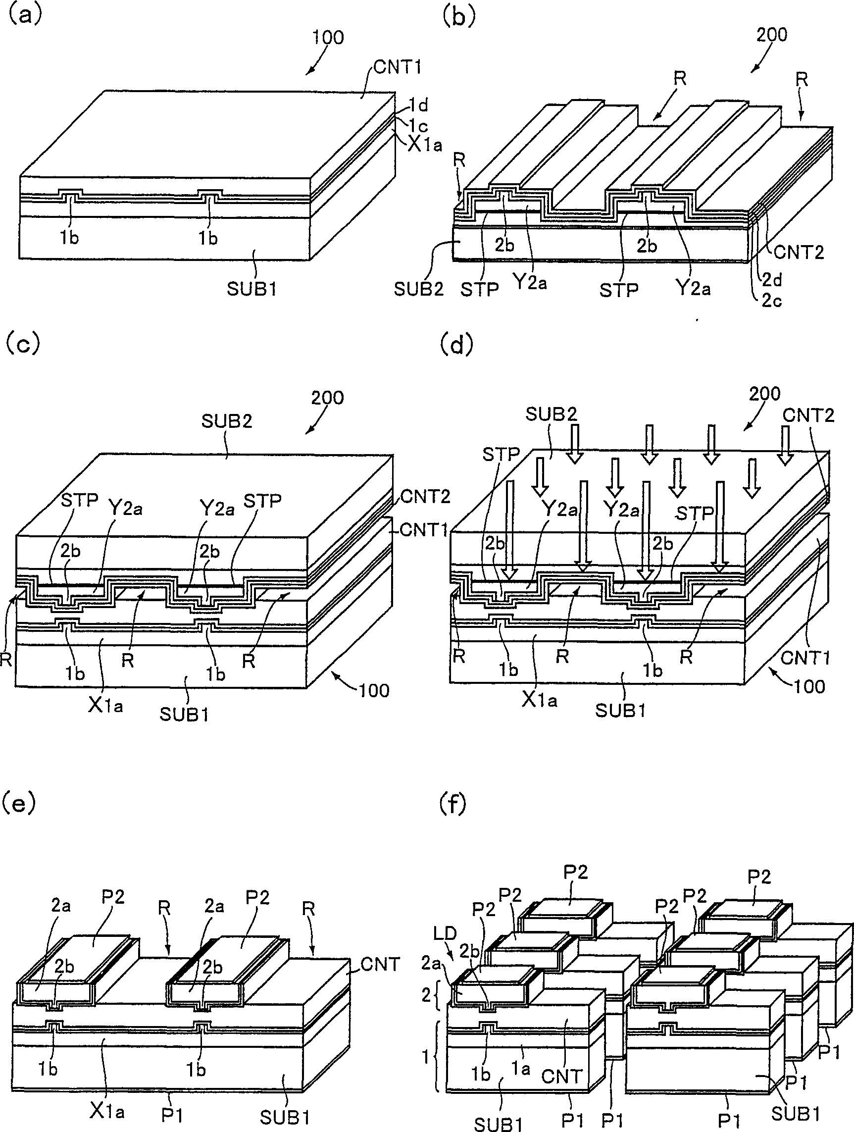
[0090] Below, refer to Figure 4 ~ Figure 7 A specific example of the first embodiment will be described. Figure 4 A schematic cross-sectional view showing the structure of a semiconductor laser fabricated according to this embodiment, Figure 5 ~ Figure 7 A schematic diagram showing a method of manufacturing the semiconductor laser device of this embodiment. and, in Figure 4 ~ Figure 7 , use the same symbols to denote and figure 1 and figure 2 same or equivalent parts.

[0091] exist Figure 4 Among them, the semiconductor laser device LD manufactured according to this embodiment includes: a first light-emitting element 1 having a first laser resonator 1a formed on a semiconductor substrate SUB1; and a second light-emitting element 2 having a second laser resonator 2a, The first and second light emitting elements 1 and 2 are fixed and bonded integrally by an adhesive layer CNT made of a welded metal (for example, Sn).

[0092] The first laser resonator 1a has an n-typ...


PUM

PropertyMeasurementUnit
thicknessaaaaaaaaaa
thicknessaaaaaaaaaa

Abstract

A process for fabricating a multi-wavelength semiconductor laser device exhibiting on excellent mass productivity. A first intermediate product is produced by forming a first multilayer laser oscillating section (1a) and a metal bonding layer on a semiconductor substrate SUB1, and a second intermediate product is produced by forming a second multilayer laser oscillating section (2a) smaller than the first laser oscillating section (1a) and a metal bonding layer that forms a trench contiguous thereto on a supporting substrate. Adhesive layers of the first and second intermediate products are fused together by bringing waveguides (1b, 2b) into close proximity thus producing an integrated adhesive layer CNT. After the first and second oscillating section (1a, 2a) are fixed, the supporting substrate is stripped from the second laser oscillating section (2a) to expose the adhesive layer CNT partially, thus fabricating a semiconductor laser device LD where the exposed adhesive layer CNT serves as a common electrode.

Description

technical field [0001] The present invention relates to a method of manufacturing a semiconductor laser device emitting a plurality of laser lights of different wavelengths. Background technique [0002] With the popularization of digital broadcasting and broadband, we have ushered in an era in which a large amount of digital content floods homes, etc., and further high-density information recording is required. In the optical disc storage system, high density has progressed from a CD (Compact Disc) with a capacity of 700 MB using light with a wavelength of 780 nm to a DVD (Digital Versatile Disc) with a capacity of 4.7 GB using light with a wavelength of 650 nm. Especially recently, an optical disc system with a capacity exceeding 20 GB has been realized using light having a wavelength of 405 nm. [0003] In such a high-density recording system, it is necessary to maintain compatibility with DVD, which has been widely used until now, so a laser with a wavelength of 650nm m...

Claims


Application Information

Patent Timeline
Patent Type & Authority Applications(China)
IPC IPC(8): H01S5/22H01S5/02H01S5/042H01S5/40
CPCH01S5/4043H01S5/0425H01S5/22H01S5/4087H01S5/0217H01S5/0216H01S5/00
Inventor 宫地护木村义则竹间清文
Owner PIONEER CORP
Why Eureka
Try Eureka