Non-polarized composite gallium nitride base substrate and production method

A GaN-based, non-polarized technology, applied in electrical components, circuits, semiconductor devices, etc., can solve the problems of heat dissipation of high-power devices, easy breakdown of devices, and reduction of internal quantum efficiency of GaN-based devices. To achieve the effect of high heat transfer efficiency

Inactive Publication Date: 2006-10-11
INVENLUX OPTOELECTRONICS (CHINA) CO LTD
View PDF5 Cites 0 Cited by
  • Summary
  • Abstract
  • Description
  • Claims
  • Application Information

AI Technical Summary

Problems solved by technology

However, there are the following disadvantages: (1) There is a built-in polarization electric field in the GaN-based epitaxial layer, which reduces the combination efficiency of electrons and holes in the GaN-based epitaxial layer, thus reducing the GaN-based epitaxial layer. The internal quantum efficiency of the device
(2) Sapphire is a mater

Method used


Image

  • Non-polarized composite gallium nitride base substrate and production method
  • Non-polarized composite gallium nitride base substrate and production method
  • Non-polarized composite gallium nitride base substrate and production method

Examples


example

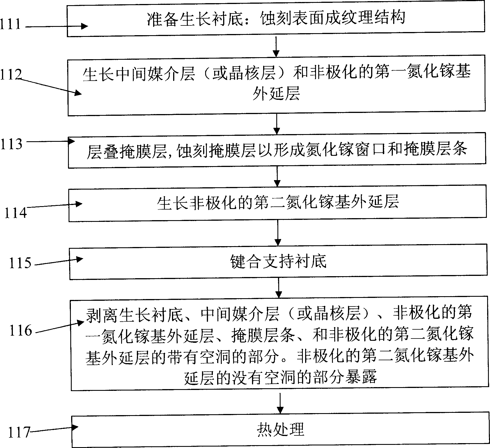
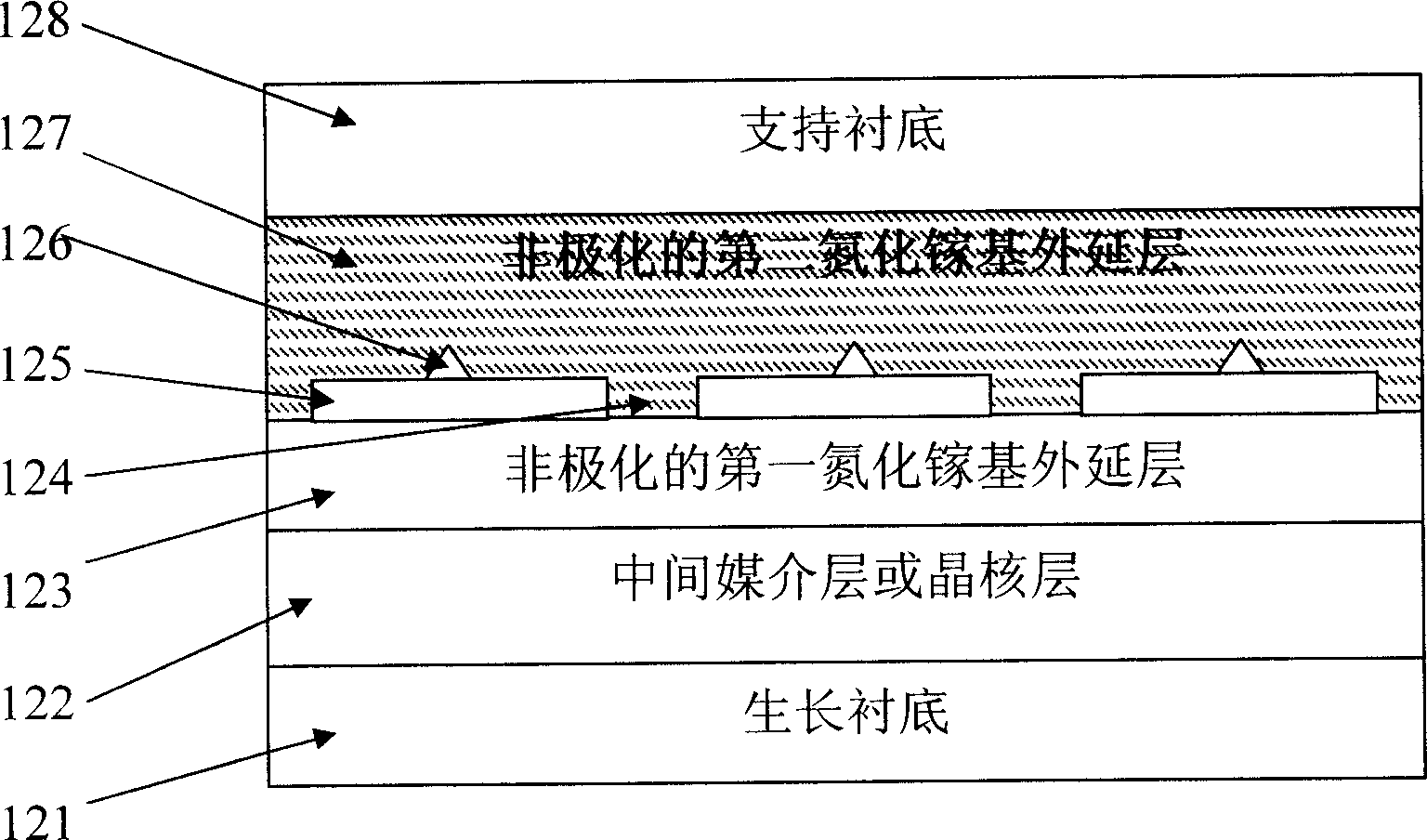
[0047] The first specific implementation example of the process flow step 112: using MOCVD, grow a layer of gallium nitride substrate with a thickness between 1 nm and 90 nm on the r-plane sapphire growth substrate (at a temperature of 400-900 ° C). Nucleation layer. The material of the crystal nucleus layer includes, but is not limited to, gallium nitride. An a-plane non-polarized first GaN-based epitaxial layer is grown on the crystal nucleus layer. A specific implementation example of growing a non-polarized a-plane first gallium nitride-based epitaxial layer: growing a non-polarized a-plane at a temperature above about 1000° C. and at a pressure less than 1 atmosphere, with an appropriate V / III ratio The thickness of the first GaN-based epitaxial layer is 1-5 microns.

[0048] A second specific implementation example of process flow step 112: using MBE, grow an aluminum nitride buffer layer on an m-plane 6H-silicon carbide growth substrate, and then grow an m-plane first...


PUM


Abstract

The disclosed non-polar composite GaN-based substrate comprises overlays between the substrate and the GaN extension layer reflection/ohm/stress buffer layer. Wherein, the preparation method for the substrate comprises: on the growth substrate, growing middle medium layer (or crystal kernel) and the non-polar first GaN-based extension layer in turn; overlaying the mask layer; etching the mask to form the GaN window and mask layer strip; growing the non-polar second GaN extension layer; overlaying the reflection/ohm/stress buffer layer; bonding substrate; peeling the substrate, medium layer, the first extension layer, mask strip, and the part with hole on the second extension layer; exposing other part of the second extension layer for thermal treatment.

Description

technical field [0001] The invention discloses a non-polar compound gallium nitride base substrate, which belongs to the technical field of semiconductor electronics. Background technique [0002] Currently, in industry, c-sapphire substrate is used as one of the main growth substrates for growing GaN-based devices (including GaN-based LEDs). However, there are the following disadvantages: (1) There is a built-in polarization electric field in the GaN-based epitaxial layer, which reduces the combination efficiency of electrons and holes in the GaN-based epitaxial layer, thus reducing the GaN-based epitaxial layer. The internal quantum efficiency of the device. (2) Sapphire is a material with low thermal conductivity, and the heat dissipation problem of high-power devices needs to be solved. [0003] In order to overcome the above-mentioned deficiencies, industries and research institutions adopt the following schemes. (1) In order to eliminate the built-in polarization el...

Claims


Application Information

Patent Timeline
IPC IPC(8): H01L33/00H01L21/18H01L21/20H01L33/02
Inventor 彭晖
Owner INVENLUX OPTOELECTRONICS (CHINA) CO LTD
Why Eureka
Try Eureka