
Non-polarized composite gallium nitride substrate lining and production method

A GaN-based, non-polarized technology, used in electrical components, semiconductor/solid-state device manufacturing, circuits, etc., can solve the problem of heat dissipation of high-power devices, easy breakdown of devices, and reduce the electron and Hole binding efficiency and other issues, to achieve the effect of high heat conduction efficiency

Inactive Publication Date: 2006-10-25
金芃 +1
View PDF5 Cites 3 Cited by
  • Summary
  • Abstract
  • Description
  • Claims
  • Application Information

AI Technical Summary

Problems solved by technology

However, there are the following disadvantages: (1) There is a built-in polarization electric field in the GaN-based epitaxial layer, which reduces the combination efficiency of electrons and holes in the GaN-based epitaxial layer, thus reducing the GaN-based epitaxial layer. The internal quantum efficiency of the device
(2) Sapphire is a material with low thermal conductivity, and the heat dissipation problem of high-power devices needs to be solved
[0004] However, the disadvantage of the lateral epitaxy method in scheme (1) is that there are voids in the gallium nitride-based epitaxial layer, which is easy to deform at high temperature, and the device is easy to be broken down, etc.

Method used


Image

  • Non-polarized composite gallium nitride substrate lining and production method
  • Non-polarized composite gallium nitride substrate lining and production method
  • Non-polarized composite gallium nitride substrate lining and production method

Examples


example

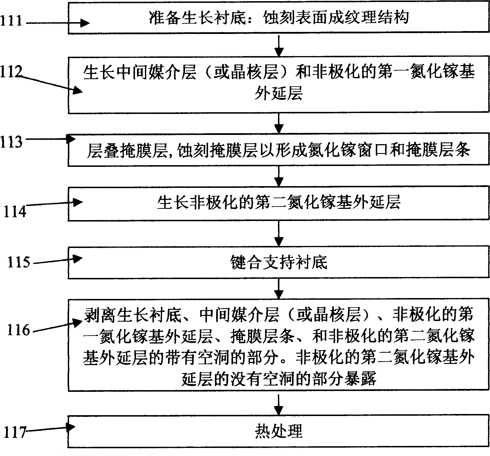
[0047] The first specific implementation example of the process flow step 112: using MOCVD, grow a layer of gallium nitride substrate with a thickness between 1 nm and 90 nm on the r-plane sapphire growth substrate (at a temperature of 400-900 ° C). Nucleation layer. The material of the crystal nucleus layer includes, but is not limited to, gallium nitride. An a-plane non-polarized first GaN-based epitaxial layer is grown on the crystal nucleus layer. A specific implementation example of growing a non-polarized a-plane first gallium nitride-based epitaxial layer: growing a non-polarized a-plane at a temperature above about 1000° C. and at a pressure less than 1 atmosphere, with an appropriate V / III ratio The thickness of the first GaN-based epitaxial layer is 1-5 microns.

[0048] A second specific implementation example of process flow step 112: using MBE, grow an aluminum nitride buffer layer on an m-plane 6H-silicon carbide growth substrate, and then grow an m-plane first...


PUM


Abstract

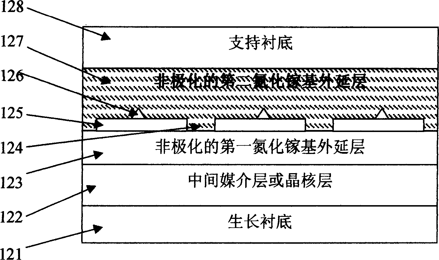
This invention discloses a method for producing a non-polar compound GaN base substrate, in which, the structure of the substrate is reflection / ohm / stress buffer layer laminated between a support substrate and non-polar GaN base epitaxial layer, the method includes: growing an intermediate layer( or a germ layer) and a non-polar first GaN base epitaxial layer orderly on the substrate, laminating a mask layer, etching the mask layer to form a GaN window and mask layer strips, growing a non-polar second GaN base epitaxial layer, laminating the reflection / ohm / stress buffer layer, bonding the support substrate, peeling off the growing substrate, the intermediate layer, the non-polar first GaN base epitaxial layer, the mask layer strips and the cavity part in the non-polar second GaN base epitaxial layer and exposing the part without cavities to be heat-processed.

Description

technical field [0001] The invention discloses a non-polar compound gallium nitride base substrate, which belongs to the technical field of semiconductor electronics. Background technique [0002] Currently, in industry, c-sapphire substrate is used as one of the main growth substrates for growing GaN-based devices (including GaN-based LEDs). However, there are the following disadvantages: (1) There is a built-in polarization electric field in the GaN-based epitaxial layer, which reduces the combination efficiency of electrons and holes in the GaN-based epitaxial layer, thus reducing the GaN-based epitaxial layer. The internal quantum efficiency of the device. (2) Sapphire is a material with low thermal conductivity, and the heat dissipation problem of high-power devices needs to be solved. [0003] In order to overcome the above-mentioned deficiencies, industries and research institutions adopt the following schemes. (1) In order to eliminate the built-in polarization el...

Claims


Application Information

Patent Timeline
IPC IPC(8): H01L21/20H01L33/00H01L33/04H01L33/32
Inventor 彭晖
Owner 金芃
Learn More