Method for manufacturing a semiconductor device

一种半导体、控制栅的技术,应用在半导体器件、半导体/固态器件制造、电固体器件等方向,能够解决不能内置所需容量、增加芯片尺寸、不能应用高存储器集成度等问题

Active Publication Date: 2006-11-01
KEY FOUNDRY CO LTD
View PDF0 Cites 12 Cited by
  • Summary
  • Abstract
  • Description
  • Claims
  • Application Information

AI Technical Summary

Problems solved by technology

However, because EEPROM cells are much larger than conventional mask ROM devices, not only cannot the required capacity be built in, but also generally increase the chip size
Therefore, the method of implementing a mask ROM device by using EEPROM cells cannot be applied to products requiring high memory integration

Method used


Image

  • Method for manufacturing a semiconductor device
  • Method for manufacturing a semiconductor device
  • Method for manufacturing a semiconductor device

Examples


Embodiment Construction

[0011] Hereinafter, a detailed description of preferred embodiments of the present invention will be provided with reference to the accompanying drawings.

[0012] Figure 1 to Figure 11 is a cross-sectional view illustrating a method for fabricating a semiconductor device according to certain embodiments of the present invention.

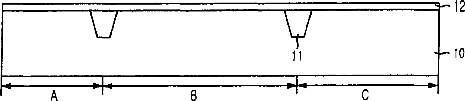
[0013] First, if figure 1 As shown, a substrate 10 is provided, which is defined as: a peripheral circuit area, in which logic devices will be formed (hereinafter referred to as "first area A"); an electrically erasable programmable read-only memory (EEPROM) cell area, in which An EEPROM cell (hereinafter referred to as "second area B") will be formed; and a flash area in which flash memory cells will be formed (hereinafter referred to as "third area C").

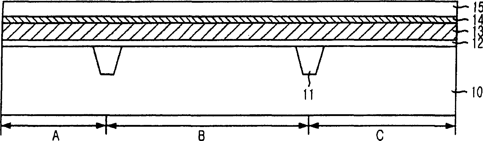
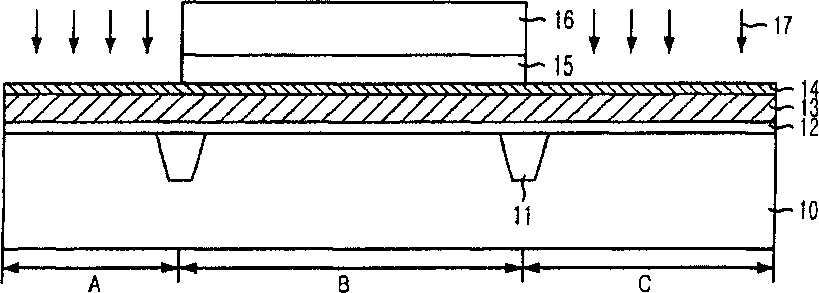
[0014] Next, a plurality of device isolation layers 11 are formed to isolate the first region A, the second region B and the third region C from each other. At this time, the device isolation...


PUM


Abstract

A method for fabricating a semiconductor device for a system on chip (SOC) for embodying a transistor for a logic device, an electrical erasable programmable read only memory (EEPROM) cell and a flash memory cell in one chip is provided. Floating gates of the EEPROM cell and the flash memory cell are formed by using a first polysilicon layer; and a gate electrode of the logic device and control gates of the EEPROM cell and the flash memory cell are formed by using a second polysilicon layer. Thus, it is possible to stably form the logic device, the EEPROM cell and the flash memory cell in one chip.

Description

technical field [0001] The present invention relates to a method for manufacturing a semiconductor device; more particularly, to a method for manufacturing a semiconductor device for a system on chip (SOC) for implementing transistors for logic devices, electrical Erasable programmable read-only memory (EEPROM) cells and flash memory cells. Background technique [0002] Recently, a smart card including multiple functions of an identification card, a credit card and electronic money in one card is widely used. The smart card not only stores user information and transaction information, but also carries programs suitable for its use. Therefore, a nonvolatile memory device for writing and storing user information and transaction information and a mask ROM device for encoding a predetermined program are constructed as a single-chip type in the smart card. For example, in the case of an integrated circuit (IC) card, such as a smart card, a mask ROM device is used as a system me...

Claims


Application Information

Patent Timeline
Patent Type & Authority Applications(China)
IPC IPC(8): H01L21/822H01L21/8247
CPCH01L27/105H10B41/43H10B41/40H10B69/00H10B41/30H01L29/40114H01L21/823437H01L21/823468
Inventor 郑涌植
Owner KEY FOUNDRY CO LTD
Why Eureka
Try Eureka