
Method for making complicate three dimension microstructure or micro device at low cost

A micro-device, low-cost technology, applied in the manufacture of micro-structure devices, micro-structure technology, micro-structure devices, etc. Problems such as the realization and popularization of complex MEMS, the design of MEMS and functional realization obstacles, etc., to achieve the effect of not being constrained by complex geometric shapes, high aspect ratio, and low cost

Inactive Publication Date: 2006-11-08
XI AN JIAOTONG UNIV
View PDF0 Cites 20 Cited by
  • Summary
  • Abstract
  • Description
  • Claims
  • Application Information

AI Technical Summary

Problems solved by technology

Although there are various microfabrication methods at present, these processes have a common defect-the fabrication of multilayer complex three-dimensional microstructures or microdevices cannot be realized at low cost, which brings great challenges to the design and function realization of microelectromechanical systems. Obstacles restricting the realization and popularization of RF MEMS devices, MOEMS devices and complex micro-electro-mechanical systems

Method used


Image

  • Method for making complicate three dimension microstructure or micro device at low cost
  • Method for making complicate three dimension microstructure or micro device at low cost
  • Method for making complicate three dimension microstructure or micro device at low cost

Examples


Embodiment Construction

[0041] 1) Technical approaches for the fabrication of complex 3D micro-devices

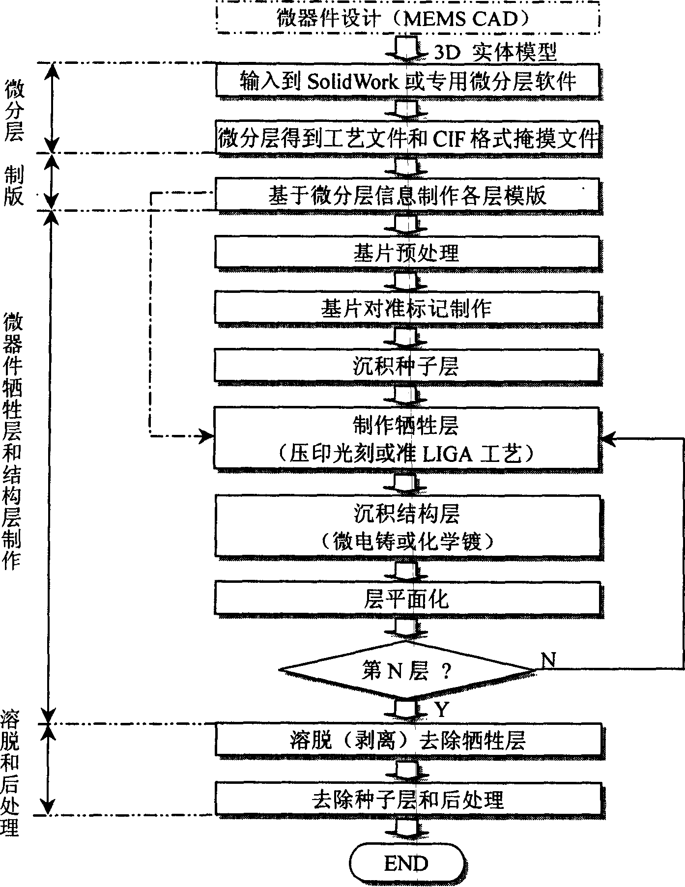
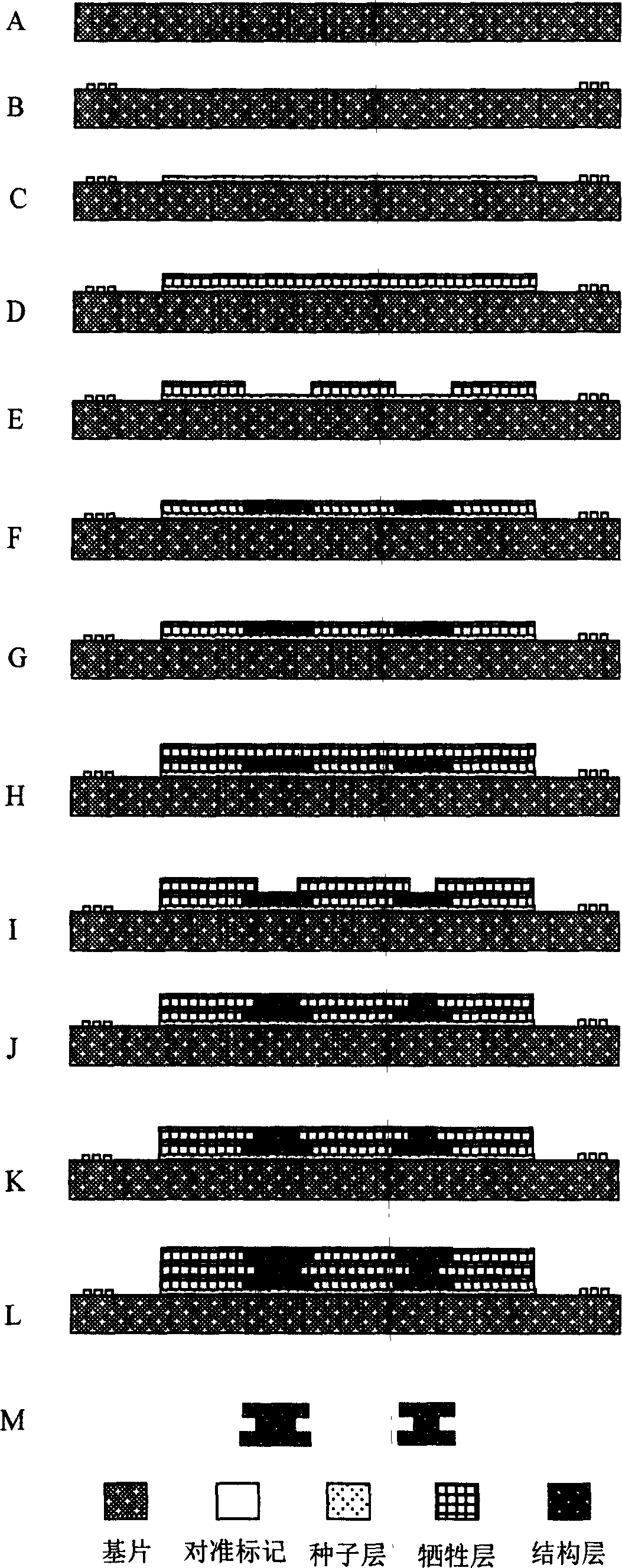
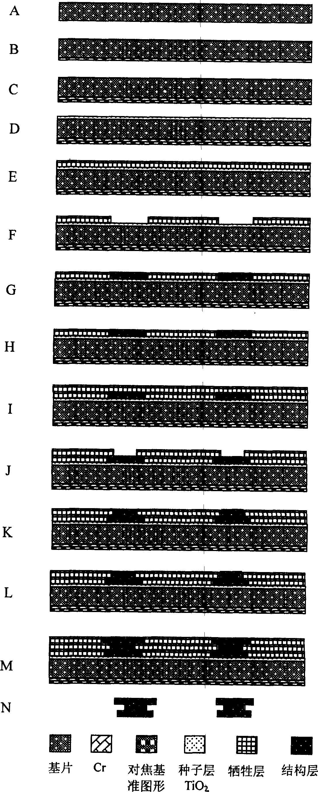
[0042] see figure 1 , the technical approach of utilizing the present invention to make complex three-dimensional micro-device is: 1. micro-layering of micro-device three-dimensional CAD solid model; 2. template making;

[0043] (1) Microlayering of 3D CAD solid model

[0044] Use software such as SolidWorks (or special software) to decompose according to the three-dimensional geometric structure characteristics of the micro-device according to the processing layer, discretize the three-dimensional CAD solid model of the micro-device along the Z direction, and divide it into two-dimensional thin layers with a certain thickness, and obtain each layer The geometric data information of the cross-section generates process data and CIF format mask files, and completes the conversion from three-dimensional entities to two-dimensional template data (MEMS process planning software can be used).

[0045]...


PUM


Abstract

The method of making complicate 3D micro device or 3D micro structure at low cost based on lamination manufacture principle combines ultraviolet impression photoetching, micro electrochemical processing, sacrificial layer and other micro processing techniques. The whole technological process includes 3D CAD solid model micro lamination of micro device, template making, multilayer micro device sacrificial layer and structural layer making, dissolving and post-treatment. The method is suitable for making complicate 3D micro device of metal material and multilayer micro device of composite material, including RF MEMS device of high conductivity material, adjustable capacity, solenoid, etc. The method has the features of low cost, high precision, compatibility with integrated circuit technology and no constraint of complicated geometric shape.

Description

technical field [0001] The invention belongs to the technical field of microfabrication and micro-nano device manufacturing, and relates to microfabrication technologies such as ultraviolet imprint lithography (or quasi-LIGA), lamination manufacturing, micro-electrochemical processing, sacrificial layer and stripping, and particularly relates to a low-cost Methods for fabricating complex three-dimensional microstructures or microdevices. Background technique [0002] The micromachining of complex three-dimensional microstructures is the key and core technology to realize microsensors, microactuators, micro-electromechanical systems (MEMS) and micro-opto-electromechanical systems (MOEMS). Electromechanical system development applications and bottlenecks in microfabrication technology. At present, there are mainly three kinds of microfabrication technologies used to manufacture microelectromechanical systems (MEMS) or microdevices: the first technology...

Claims


Application Information

Patent Timeline
IPC IPC(8): B81C1/00
Inventor 兰红波丁玉成刘红忠卢秉恒
Owner XI AN JIAOTONG UNIV
Learn More