Trench etching method

A trench and etching rate technology, which is applied in the manufacture of electrical components, circuits, semiconductors/solid-state devices, etc., can solve the problems of Poly affecting the trench etching atmosphere, poor etching selectivity, and inapplicability, so as to eliminate Adverse effects, improvement of trench etching quality, and effects of preventing abnormalities

Active Publication Date: 2020-07-10
SHANGHAI HUAHONG GRACE SEMICON MFG CORP
View PDF5 Cites 0 Cited by
  • Summary
  • Abstract
  • Description
  • Claims
  • Application Information

AI Technical Summary

Problems solved by technology

But in the deep trench etching scenario, there are many limitations
The HM of the deep trench has requirements on the shape, so its etching has a poor selection ratio for Oxide and Nitride, and Nitride is not suitable for growing too thick, so it is not applicable
[0005] The selection ratio of polysilicon (Poly)

Method used


Image

  • Trench etching method
  • Trench etching method
  • Trench etching method

Examples


Embodiment Construction

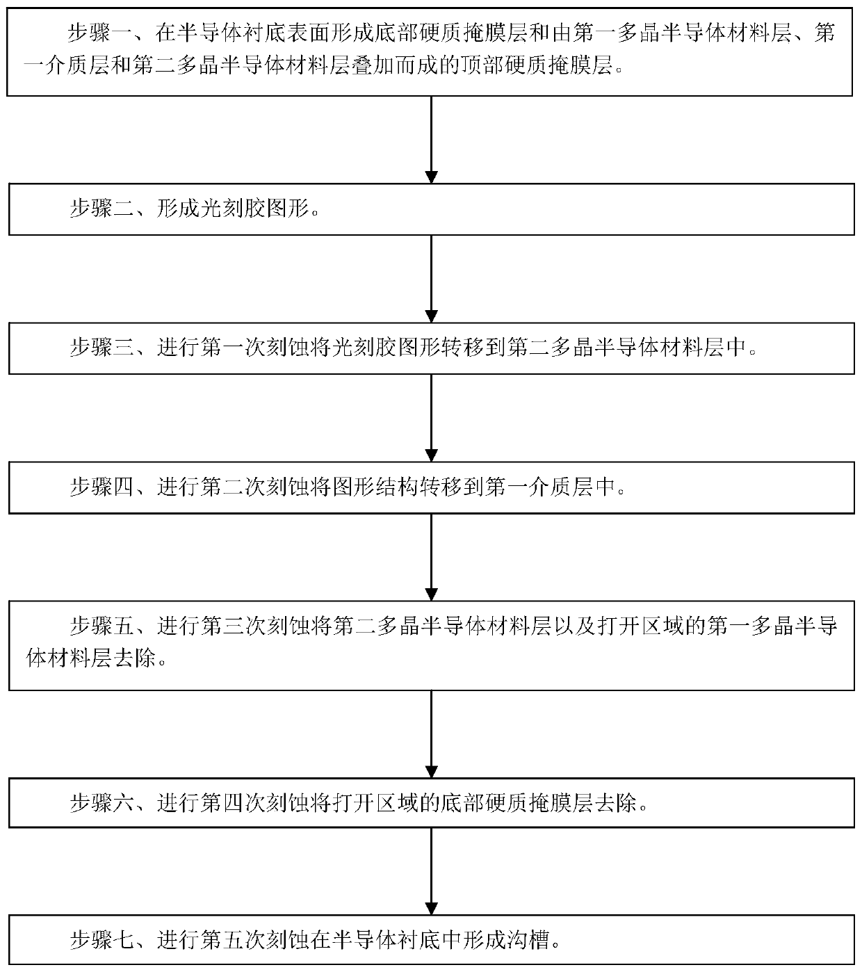
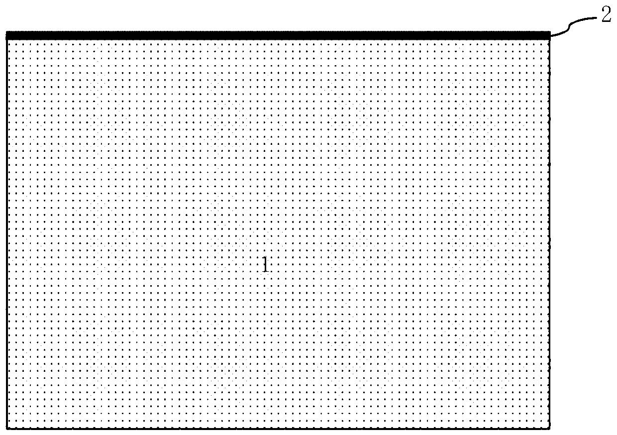
[0042] Such as figure 1 Shown is the flow chart of the etching method of the groove of the embodiment of the present invention; Figure 2A to Figure 2M Shown is a schematic diagram of the device structure in each step of the trench etching method of the embodiment of the present invention; the trench etching method of the embodiment of the present invention includes the following steps:

[0043] Step 1, such as Figure 2A As shown, a semiconductor substrate 1 for forming trenches 7 is provided, and a bottom hard mask layer 2 is formed on the surface of the semiconductor substrate 1 .

[0044] Such as Figure 2B As shown, a first polycrystalline semiconductor material layer 3 is formed on the surface of the bottom hard mask layer 2 .

[0045] Such as Figure 2C As shown, a first dielectric layer 4 is formed on the surface of the first polycrystalline semiconductor material layer 3 .

[0046] Such as Figure 2D As shown, a second polycrystalline semiconductor material laye...


PUM

PropertyMeasurementUnit
Thicknessaaaaaaaaaa

Abstract

The invention discloses a trench etching method. The trench etching method comprises the following steps: forming a bottom hard mask layer and a top hard mask layer on the surface of a semiconductor substrate, wherein the top hard mask layer is formed by superposing a first polycrystalline semiconductor material layer, a first dielectric layer and a second polycrystalline semiconductor material layer; forming a photoresist pattern; etching for the first time to transfer the photoresist pattern into the second polycrystalline semiconductor material layer; etching for the second time to transferthe pattern structure into the first dielectric layer; etching for the third time to remove the second polycrystalline semiconductor material layer and the first polycrystalline semiconductor material layer in the opening area; etching for the fourth time to remove the hard mask layer at the bottom of the open area; and etching for the fifth time to form a trench in the semiconductor substrate. According to the invention, the thickness of the photoresist can be reduced, so that the opening width of the groove can be reduced, the opening size of the groove can be accurately controlled, and meanwhile, the thickness of the hard mask layer can be increased, so that the depth of the groove can be increased.

Description

technical field [0001] The invention relates to a method for manufacturing a semiconductor integrated circuit, in particular to a groove etching method. Background technique [0002] The depth of trenches in super junction devices or deep trench capacitive devices often reaches tens of microns, so the trenches of super junction devices or deep trench capacitive devices are usually also called deep trenches. In application scenarios such as super junction devices or deep trench capacitor devices, the etching of deep trenches is a critical and even decisive process. Deep trenches are usually formed in semiconductor substrates such as silicon substrates. Deep trenches are usually realized by etching silicon on the silicon substrate. In order to etch the silicon substrate, it is usually necessary to etch the silicon substrate A hard mask layer (HM) is formed on the surface. In the existing methods, an oxide layer (Oxide), a nitride layer (Nitride) and an oxide layer (ONO) or a ...

Claims


Application Information

Patent Timeline
IPC IPC(8): H01L21/308
CPCH01L21/3081H01L21/3085H01L21/3086H01L21/3088
Inventor 李昊
Owner SHANGHAI HUAHONG GRACE SEMICON MFG CORP
Why Eureka
Try Eureka