

Method for preparing films of cobalt silicate
A technology of cobalt silicide and thin film, which is applied in the field of preparation of cobalt silicide thin film, and can solve the problems of poor thermal stability and limitation of thin film
- Summary
- Abstract
- Description
- Claims
- Application Information
AI Technical Summary
Problems solved by technology
Method used
Image

Examples
Embodiment Construction
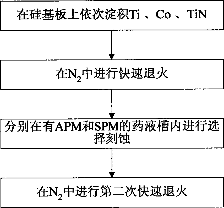
[0013] Such as figure 1 As shown, a method for preparing a cobalt silicide thin film of the present invention includes the following steps. First, Ti with a thickness of 25-45 Ȧ and a thickness of 70-150 Ȧ are respectively deposited on a silicon substrate with a 100-crystal orientation by physical vapor deposition. Co and TiN with a thickness of 80-200 Ȧ; followed by pure N at 5slm 2 The medium temperature is 580-700°C, and the process time is 60-120S for rapid annealing; again in the mixed solution of ammonium hydroxide, hydrogen peroxide and deionized water (NH 4 OH:H 2 o 2 :H 2 O=1:5:5, referred to as APM) and sulfuric acid and hydrogen peroxide mixed solution (H 2 SO 4 :H 2 o 2 =4:1, referred to as SPM) for selective etching in the chemical solution tank; finally, perform the second rapid annealing in 5slm pure N2, the temperature is 825-900°C, and the process time is 30-60S.
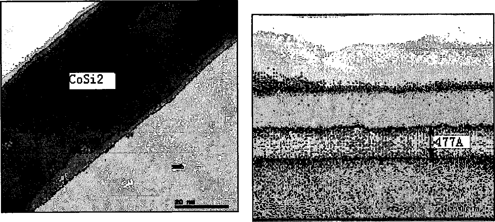
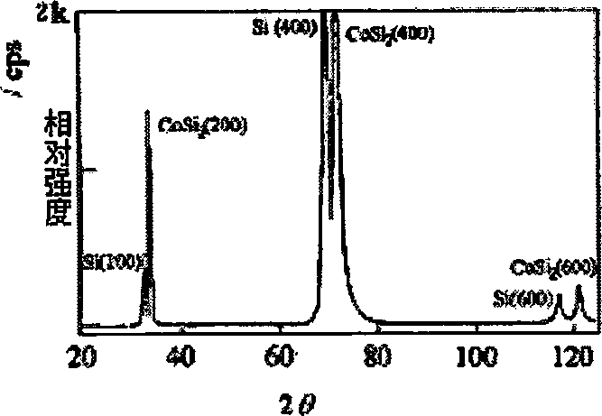
[0014] CoSi produced by a method for preparing a cobalt silicide thin film according to ...
PUM
 Abstract
Description
Claims
Application Information