Communication circuit module

A communication circuit and circuit technology, applied to printed circuit components, circuit layout on support structures, including printed electrical components, etc., can solve problems such as reducing the efficiency of high-frequency circuit modules, serious parasitic effects, and inability to reduce line widths. , to prevent and interfere with each other, reduce the thickness of each layer, and reduce the size

Inactive Publication Date: 2007-01-10
DELTA ELECTRONICS INC
View PDF0 Cites 0 Cited by
  • Summary
  • Abstract
  • Description
  • Claims
  • Application Information

AI Technical Summary

Problems solved by technology

On the other hand, for the microstrip line 204a in the circuit structure 204, since there are disconnected ground planes 203 and 202 above and below it, and both the upper and lower substrates have a high dielectric constant ε1, so The electric field densely exists on both sides of the microstrip line 204a, which will lead to very large parasitic capacitance
[0006] In addition, if you want to form more layers of circuit structures, since a ground plane may be formed between each circuit structure to provide shielding effect, the parasitic effect will be more serious, which will greatly reduce the performance of high-frequency circuit modules.
Although reducing the line width of the microstrip line can reduce the parasitic capacitance, since the current manufacturing process technology cannot reduce the line width without limit, how to reduce the microstrip line width without reducing the line width of the microstrip line The parasitic capacitance of the current high-frequency circuit designers has become an urgent goal to achieve

Method used


Image

  • Communication circuit module
  • Communication circuit module
  • Communication circuit module

Examples


Embodiment Construction

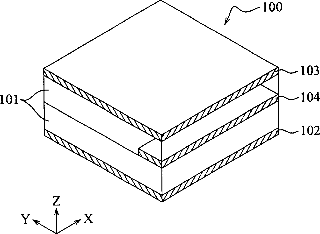
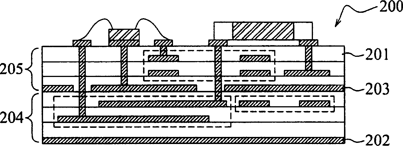
[0019] Figure 4 It is a cross-sectional view of a communication circuit module 400 according to an embodiment of the present invention. Figure 5 for Figure 4 Schematic diagram of the electric field distribution in . Please refer to Figure 4 The communication circuit module 400 is composed of a circuit area 402 and a barrier layer 404 , wherein the dielectric constant value of the barrier layer 404 is lower than the dielectric constant value of the substrate 420 of the circuit area 402 . The communication circuit module 400 may be a high frequency circuit module, a bluetooth module or a wireless communication module.

[0020] The circuit area 402 is formed by stacking several layers of substrates 420 and has circuit structures 410 , 412 and a ground plane 406 . The material of the substrate 420 can be low dielectric constant material, ceramic material, organic polymer material, silicon material or high dielectric constant material. Ground plane 406 is located between c...


PUM


Abstract

The module of communication circuit possesses at least a first circuit structure, at least a second circuit structure, at least a barrier layer, at least a first grounding plane, at least a second grounding plane. The first circuit structure is located at least a first base plate. The second circuit structure is located at least a second base plate. The first base plate and the second base plate form a stack base plate. One side of the barrier layer is contacted to the stack base plate. Value of dielectric constant of the barrier layer is lower than values of dielectric constant of the first base plate and the second base plate. The first grounding plane is located between the first circuit structure and the second circuit structure. The second circuit structure is located at another side of the barrier layer. The first grounding plane is connected to the second circuit structure electrically.

Description

technical field [0001] The invention relates to a high-frequency circuit module, in particular to a high-frequency circuit module with an improved ground plane structure. Background technique [0002] In recent years, with the continuous miniaturization of various mobile communication products, the internal high-frequency circuits are also developing towards the goal of high integration. Therefore, it has become a major trend to use high dielectric materials as the substrate of the circuit structure. However, designing high-frequency circuits on high-dielectric materials presents considerable problems for designers. [0003] Specifically, as Figure 1A As shown, the known high frequency circuit structure 100 is composed of a substrate 101 including ground planes 102 and 103 and a stripline 104 in the circuit structure. The equivalent circuit diagram of this structure is shown in Figure 1B As shown, for the microstrip line 104 , there is an effect of a series inductor L a...

Claims


Application Information

Patent Timeline
IPC IPC(8): H05K7/02H05K1/16H05K1/02
Inventor 史承彦
Owner DELTA ELECTRONICS INC
Why Eureka
Try Eureka