Homogeneous-thickness silicon-phase epitaxial-layer growth device and method

A vapor phase epitaxy and growth device technology, which is applied in the directions of crystal growth, single crystal growth, single crystal growth, etc., can solve the problems of inconsistent epitaxial layer thickness, etc., and achieve the effects of avoiding temperature differences, increasing area, and simple process

Inactive Publication Date: 2007-01-17
HEBEI UNIV OF TECH
View PDF0 Cites 2 Cited by
  • Summary
  • Abstract
  • Description
  • Claims
  • Application Information

AI Technical Summary

Problems solved by technology

However, with this method, the boundary effect of gas flow and regional differences in temperature and reaction gas concentration can still cause warping of the edge of the epitaxial layer and inconsistency in the thickness of the epitaxial layer between epitaxial wafers grown on different positions of the susceptor in the same furnace

Method used


Image

  • Homogeneous-thickness silicon-phase epitaxial-layer growth device and method
  • Homogeneous-thickness silicon-phase epitaxial-layer growth device and method
  • Homogeneous-thickness silicon-phase epitaxial-layer growth device and method

Examples


Embodiment 1

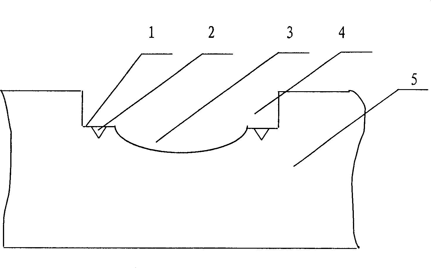
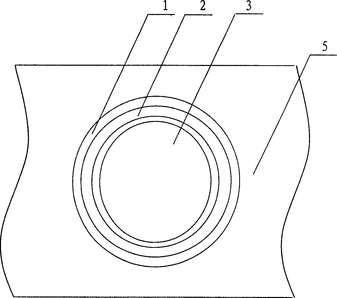
[0039] Open a φ4" placement groove on the upper surface of the graphite base, the step width in the groove is 1mm, the depth of the groove is 1mm, the depth of the arc-shaped pit is 1mm, and the upper surface of the silicon substrate is 0.1mm lower than the upper surface of the base. Use the above The graphite base is subjected to the epitaxial process according to the conventional method, and four slip lines appear on the surface of the obtained epitaxial layer, and the total length is smaller than the diameter of the silicon wafer, which meets the control requirements of the slip line.

[0040] The epitaxial layer thickness parameters are as follows:

[0041] W 上 =21.17W 中 =20.56W 下 =20.26W 左 =21.93W 右 =20.99

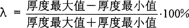
[0042] The thickness uniformity λ=3.96%, but it has not yet reached the required thickness uniformity range, so the epitaxial layer needs to be vapor-phase polished.

[0043] According to the requirements of thickness consistency, the average removal thickness i...

Embodiment 2

[0051] Open a φ4 "placement groove on the upper surface of the graphite base, the step width in the groove is 3mm, the depth of the groove is 3mm, the depth of the arc-shaped pit is 5mm, and the upper surface of the silicon substrate is 1mm lower than the upper surface of the base. The obtained epitaxial layer There is only one slip line on the surface, and the length is less than the diameter of the silicon wafer, which meets the control requirements of the slip line.

[0052] The thickness parameters of the epitaxial layer are as follows:

[0053] W 上 =20.66W 中 =20.94W 下 =21.42W 左 =22.02W 右 =21.18

[0054] Its thickness uniformity λ=3.19%, is within the required range of thickness uniformity, so it is not necessary to implement vapor phase polishing.

[0055] Using the same silicon substrate only to implement the conventional epitaxial process, more than 16 slip lines appeared on the surface of the obtained epitaxial layer, and the total length was far greater than the...

Embodiment 3

[0061] Open the φ4 "placement groove on the upper surface of the graphite base, the step width in the groove is 2mm, the depth of the groove is 2mm, the depth of the arc-shaped pit is 3mm, and the upper surface of the silicon substrate is 0.4mm lower than the upper surface of the base. The obtained epitaxy There is only one slip line on the surface of the layer, and the length is less than the diameter of the silicon wafer, which meets the control requirements of the slip line.

[0062] The thickness parameters of the epitaxial layer are as follows:

[0063] W 上 =21.00W 中 =21.17W 下 =21.77W 左 =21.80W 右 =22.26

[0064] Its thickness uniformity λ=2.91%, is within the required thickness uniformity range, so it is not necessary to implement vapor phase polishing.

[0065] Using the same silicon substrate only to implement the conventional epitaxial process, more than 20 slip lines appeared on the surface of the obtained epitaxial layer, and the total length was far greater th...


PUM

PropertyMeasurementUnit
thicknessaaaaaaaaaa
thicknessaaaaaaaaaa

Abstract

The present invention discloses a growth device and process of a silicon vapor epilayer and aims at providing a growth device and a process with homogeneous epilayer, convenient operation and high efficiency. The growth device includes a base body, a fixing slot on the base body, a step of 1-3mm wide on the edge of the fixing slot bottom, an annular groove of 1-3mm deep on the step and an arcual concave of 1-5mm deep below the step. The top of the annular groove is 1-3mm wide. The growth process includes the following steps: the silicon substrate wafer is positioned in the fixing slot with the upper surface of the substrate wafer 0.1-1mm lower than the upper surface of the base, and the epilayer grows. This invention has simple arts and crafts, provides homogeneous epilayer, controls the distribution area of the slip lines and removes the contaminative layer of metal impurities on the surface, improving the quality of the silicon epilayer and ensuring the performance of the product.

Description

technical field [0001] The invention relates to a growth method of a silicon vapor phase epitaxial layer, more specifically, relates to a growth method of a silicon vapor phase epitaxial layer which can well control the thickness uniformity. Background technique [0002] From the perspective of further improving the speed and integration of silicon ICs, silicon epitaxial wafers suitable for deep submicron processes will become the mainstream of silicon material development in the future, which puts more stringent requirements on the quality and performance of silicon epitaxial wafers . [0003] In the preparation process of silicon planar transistors and integrated circuits, the thickness consistency of the epitaxial layer directly affects the follow-up process. The inconsistency of epitaxial layer thickness is mainly manifested in: the edge of the epitaxial layer is warped, the thickness of the epitaxial layer on the entire silicon wafer is inconsistent, and the thickness ...

Claims


Application Information

Patent Timeline
Patent Type & Authority Applications(China)
IPC IPC(8): C30B25/02C30B29/06
Inventor 刘玉岭张建新黄妍妍
Owner HEBEI UNIV OF TECH
Why Eureka
Try Eureka