Method for reducing wafer harm caused by shallow slot insulation chemical mechanical polishing technique

A chemical-mechanical, wafer-based technology used in semiconductor/solid-state device manufacturing, electrical components, circuits, etc.

Active Publication Date: 2007-01-31
UNITED MICROELECTRONICS CORP
View PDF0 Cites 8 Cited by
  • Summary
  • Abstract
  • Description
  • Claims
  • Application Information

AI Technical Summary

Problems solved by technology

[0011] The main purpose of the present invention is to provide an improved manufacturing m...

Method used


Image

  • Method for reducing wafer harm caused by shallow slot insulation chemical mechanical polishing technique
  • Method for reducing wafer harm caused by shallow slot insulation chemical mechanical polishing technique
  • Method for reducing wafer harm caused by shallow slot insulation chemical mechanical polishing technique

Examples


Embodiment Construction

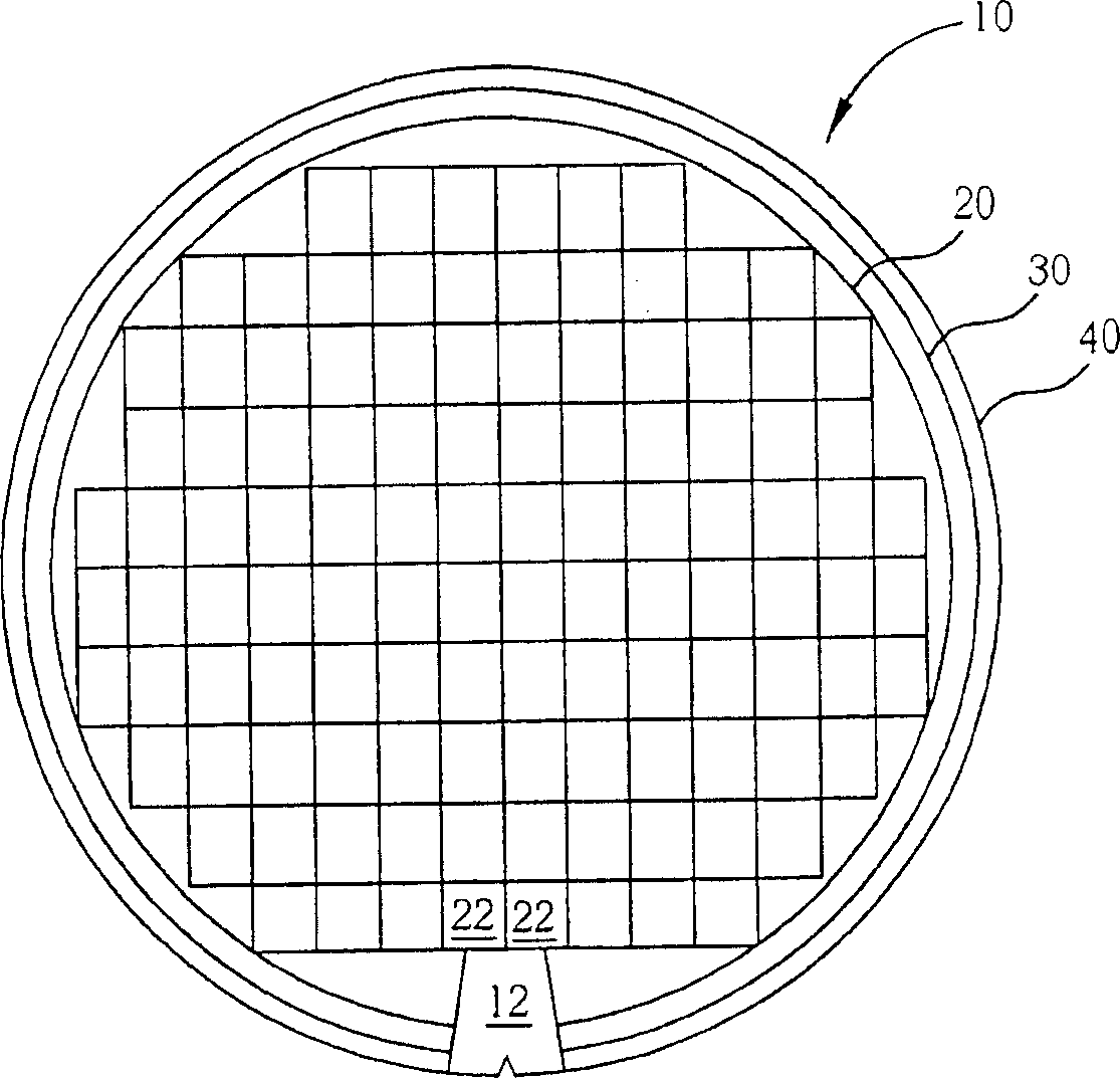
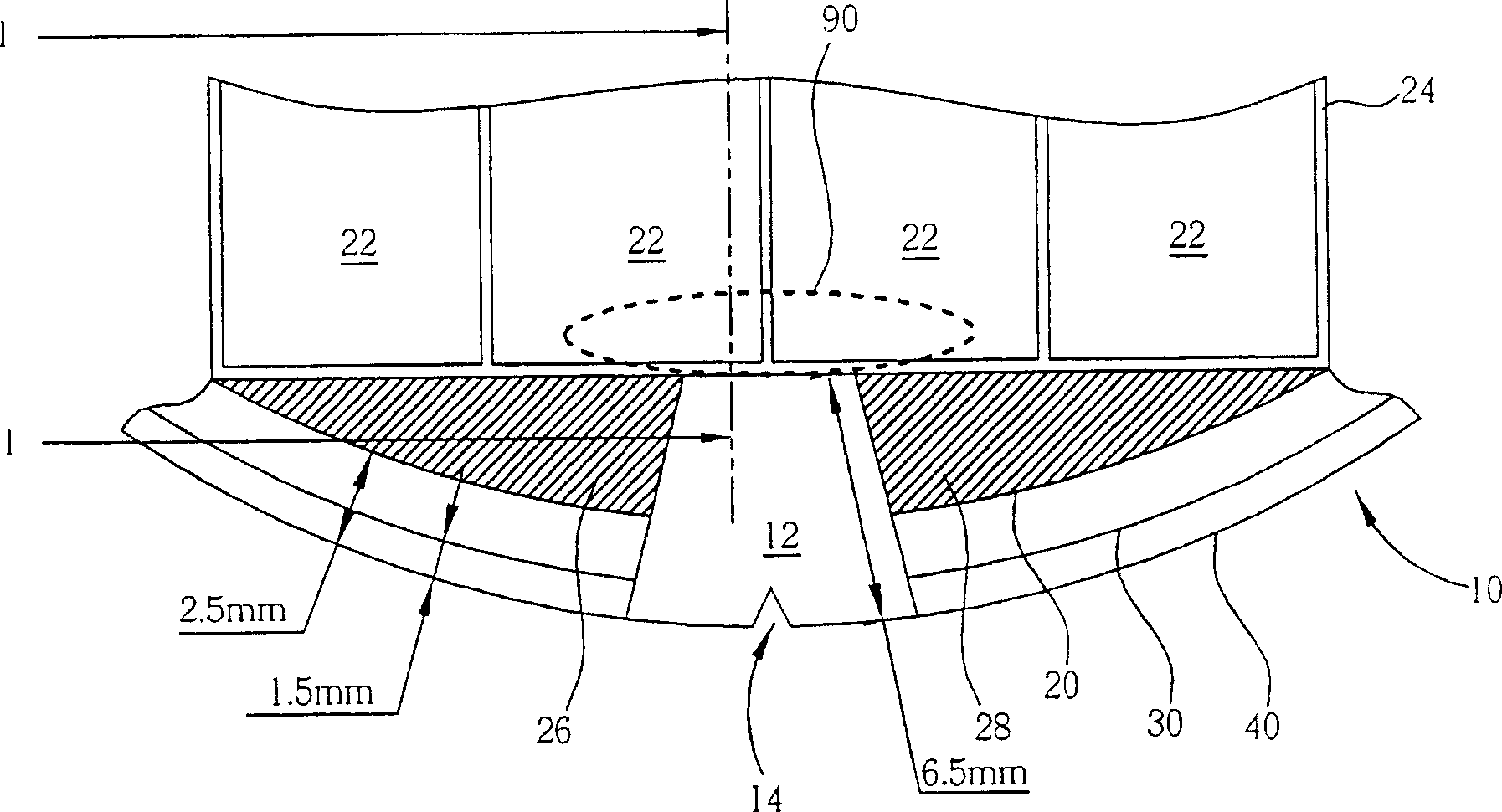
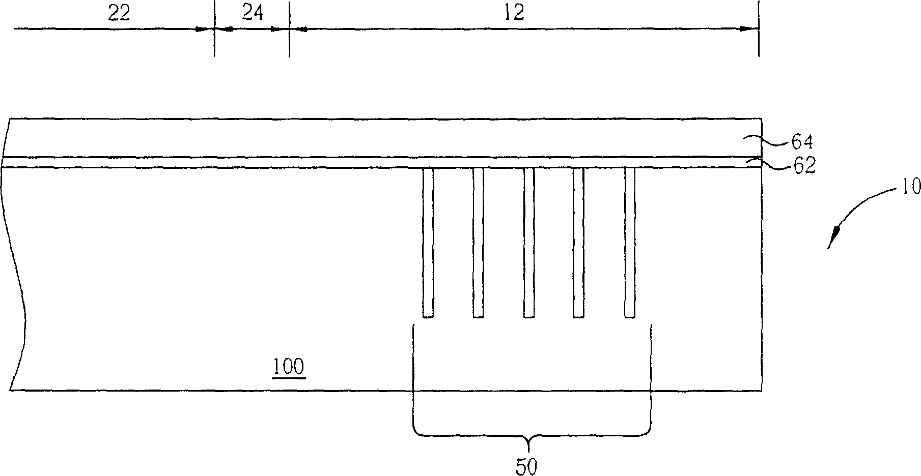
[0035] see Figure 8 , which shows the top view near the laser marking area 12 of the wafer 10 according to the preferred embodiment of the present invention, which includes the integrated circuit wafer area 22, the wafer edge exposure area (waferedge exposure, WEE) and the wafer edge cleaning area ( edge bead removal, EBR). Such as Figure 8 As shown, the wafer 10 has a V-shaped notch 14 , and the laser marking area 12 is generally located near the V-shaped notch 14 and is provided on the front side of the wafer 10 . In the laser marking area 12 , there is provided a laser marking 50 of the wafer including the batch number of the wafer and the identification number of the wafer. The laser marking area 12 is adjacent to the scribe line 24 surrounding the IC die area 22 , and the interface between the laser marking area 12 and the scribe line 24 is usually about 6.5 mm away from the edge 40 of the wafer. The purpose of the laser marking area 12 being disposed on the edge of ...


PUM


Abstract

The invention offers the method used to reduce wafer damage caused by shallow ridges insulating chemico-mechanical polishing technology. It includes the following steps: offering a wafer includes integrate circuit crystal area, cutting way, and laser number graving area; forming active area photoresist pattern includes trench opening and nominal opening; etching bedding and substrate to form isolating shallow ridge and nominal shallow ridge; depositing trench filler material and filling the isolating and nominal shallow ridges; chemico-mechanical polishing until the bedding.

Description

technical field [0001] The invention relates to the field of semiconductor technology, in particular to a semiconductor technology method capable of reducing wafer damage caused by a shallow trench insulation chemical mechanical polishing process, thereby improving yield. Background technique [0002] As is well known to those skilled in the art, semiconductor integrated circuits are made on the surface of semiconductor wafers such as monocrystalline silicon wafers, and the surface of the wafer is usually divided into different crystal square areas by partitions, and each crystal square area is divided into Semiconductor processes such as photolithography and etching technology form components and circuits, and then form a single chip after testing, dicing and packaging. In semiconductor processes, such as thermal oxidation process or cleaning process, sometimes multiple wafers can be processed at the same time, also known as batch wafer processing, while in some process ste...

Claims


Application Information

Patent Timeline
IPC IPC(8): H01L21/762H01L21/3105
Inventor 张幼弟
Owner UNITED MICROELECTRONICS CORP
Why Eureka
Try Eureka