Electromagnetic wave absorber

An electromagnetic wave and absorber technology, applied in the field of laminated electromagnetic wave absorbers, can solve the problems of limited filling degree of flat soft magnetic body powder, inability to install well, and limited installation locations, and achieves excellent electromagnetic wave shielding properties and adhesion strength. Excellent effect with little temperature dependence

Inactive Publication Date: 2007-03-07
GELTEC
View PDF7 Cites 15 Cited by
  • Summary
  • Abstract
  • Description
  • Claims
  • Application Information

AI Technical Summary

Problems solved by technology

However, there is no material that has these three properties at the same time. In such an application, it is necessary to have flexibility, heat resistance, flame retardancy, etc., but there is no material that can satisfy these properties at the same time.
In particular, in the absorber that also has the function of reflecting electromagnetic waves, the installation place is limited, such as the top surface of the resin case, etc., which cannot be installed well. This is the actual situation.
[0014] In addition, no matter which technology is used, the structure of the electromagnetic wave absorber has a limitation in the degree of filling of flat soft magnetic powder and the like. With the problem
In particular, there is no material that has the same effect in the MHz to 10GHz range, and has electromagnetic wave absorption performance, high resistance, high insulation, and thermal conductivity. In this application, flexibility, heat resistance, and flame retardancy are also required. , but no material can meet these performance requirements at the same time

Method used


Image

  • Electromagnetic wave absorber
  • Electromagnetic wave absorber
  • Electromagnetic wave absorber

Examples


Embodiment 1

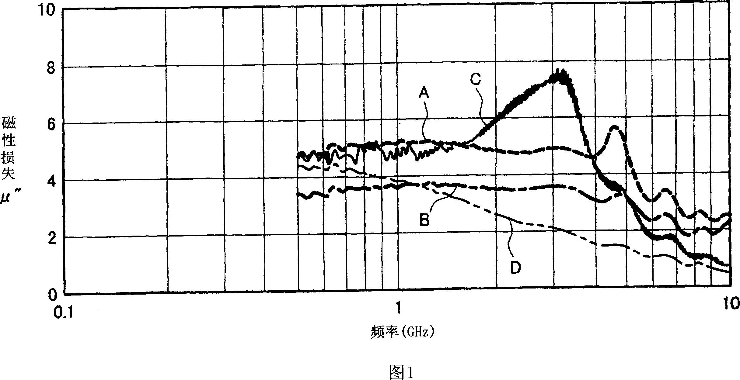
[0148] Methyltrimethoxysilane will be used for particle size distribution D 50 83% by weight of Ni-Zn soft ferrite (BSN-828 (trade name): manufactured by Toda Industry Co., Ltd.) with a surface treatment of 10 to 30 μm, particle size distribution D 50 Octahedral magnetite particles (KN-320 (trade name): manufactured by Toda Industries Co., Ltd.) of 0.1 to 0.4 μm in 5% by weight, and JIS K2207-1980 (50 g load) with a penetration of 150 Silicone gel (CF-5106 (trade name): manufactured by Toray Dow Corning Silicone Co., Ltd.) 12% by weight was mixed, vacuum degassed, and then flowed between the glass plates so as not to mix air, and Press molding was carried out by heating at 70°C for 60 minutes to obtain a molded body with a thickness of 1 mm and a smooth surface. Table 1 shows the evaluation results of the molded body.

Embodiment 2

[0150] Except for changing the compounding amount of magnetite and silicone gel to the amounts shown in Table 1, the same operation as in Example 1 was carried out to obtain a molded body, and the evaluation results of the molded body are shown in Table 1. .

Embodiment 3

[0168] Methyltrimethoxysilane will be used for particle size distribution D 50 50% by weight of Ni-Zn-based soft ferrite (BSN-714 (trade name): manufactured by Toda Kogyo Co., Ltd.) with a surface treatment of 1 to 10 μm, particle size distribution D 50 25% by weight of flat soft magnetic metal powder (JEM-M (trade name) manufactured by Jemco Co., Ltd.) with a self-oxidizing property of 0.26% by weight and a particle size distribution of 8 to 42 μm. 50 Octahedral magnetite particles (KN-320 (trade name): Toda Kogyo Co., Ltd.) 5% by weight of 0.1-0.4 μm and silicon with a penetrability of 150 according to JIS K2207-1980 (50 g load) Ketone gel (CF-5106 (trade name): manufactured by Toray Dow Corning Silicone Co., Ltd.) was mixed at 20% by weight, and after vacuum defoaming, it was poured between the glass plates so as not to mix air, and the Press molding was carried out by heating at 70°C for 60 minutes to obtain a smooth-surfaced molded body with a thickness of 1 mm. Table 2...


PUM

PropertyMeasurementUnit
specific surface areaaaaaaaaaaa
particle diameteraaaaaaaaaa
particle sizeaaaaaaaaaa

Abstract

An electromagnetic wave absorber comprising (a) soft ferrite having its surface treated with a silane compound having no functional group, (c) magnetite and (d) silicone, or comprising (a) soft ferrite having its surface treated with a silane compound having no functional group, (b) flat soft magnetic metal powder, (c) magnetite and (d) silicone, which electromagnetic wave absorber excels in electromagnetic wave absorption, heat conduction and flame resistance, exhibiting less temperature dependence, and which electromagnetic wave absorber is soft, excelling in adhesion strength and further excelling in high resistance high insulation properties and in energy conversion efficiency being stable in MHz to 10GHz broadband frequency. There is further provided a laminated electromagnetic wave absorber comprising the above electromagnetic wave absorber overlaid with a reflection layer of conductor, which laminated electromagnetic wave absorber can be closely stuck onto an unwanted electromagnetic wave emission source such as a high-speed operating device, having such an adhesive strength that even when stuck to a horizontal glassy-surface ceiling face of resin-made cage, would not fall.

Description

technical field [0001] The present invention relates to an electromagnetic wave absorber, an electromagnetic wave absorber with broadband frequency characteristics, and a laminated electromagnetic wave absorber. In particular, it relates to electromagnetic wave absorbers with excellent electromagnetic wave absorption, thermal conductivity, and flame retardancy, small temperature dependence, softness, excellent adhesion strength, high resistance and high insulation properties, and no attachment restrictions; electromagnetic wave absorbers with broadband frequency characteristics And a laminated electromagnetic wave absorber with excellent electromagnetic wave absorption and electromagnetic wave shielding properties that can be attached to the top surface of the housing and can be attached to the radiation source of unnecessary electromagnetic waves such as high-speed computing components. Background technique [0002] In recent years, with the development of electromagnetic w...

Claims


Application Information

Patent Timeline
Patent Type & Authority Applications(China)
IPC IPC(8): H05K9/00H01F1/34H01F1/36C01G49/00H01Q17/00C08L83/04C08K9/06C01G49/08H01F1/00
Inventor 小林达也
Owner GELTEC
Why Eureka
Try Eureka