
Method for making field transmitting triode

A manufacturing method and triode technology, applied in the manufacture of discharge tubes/lamps, cold cathodes, electrode systems, etc., can solve the problem of poor uniformity of aperture, distribution uniformity, and poor vertical alignment, which affects the diameter of nanometer carbon tubes Uniformity, distribution uniformity, vertical alignment, cathode line disconnection and other issues, to achieve the effect of improving tube diameter uniformity, improving field emission characteristics, and high process temperature

Inactive Publication Date: 2007-03-14
CHUNGHWA PICTURE TUBES LTD
View PDF1 Cites 2 Cited by
  • Summary
  • Abstract
  • Description
  • Claims
  • Application Information

AI Technical Summary

Problems solved by technology

However, the aluminum anodized film formed in this patented method has poor uniformity of dimension, uniformity of distribution and vertical alignment of the hole array, which further affects its The diameter uniformity, distribution uniformity and vertical alignment of nanometer carbon tubes in the hole, and affect their field emission characteristics
In addition, this patent must use aluminum or its alloys as the cathode line. Aluminum metal has a low melting point, so the subsequent process temperature must be lower than 450°C, and only a relatively low temperature chemical vapor deposition method can be used to grow carbon nanotubes.
In addition, the carbon nanotube field emission device formed by using aluminum or its alloy as the cathode line, in a high current operating environment, the cathode line is prone to electromigration and cause open circuit

Method used


Image

  • Method for making field transmitting triode
  • Method for making field transmitting triode
  • Method for making field transmitting triode

Examples


Embodiment Construction

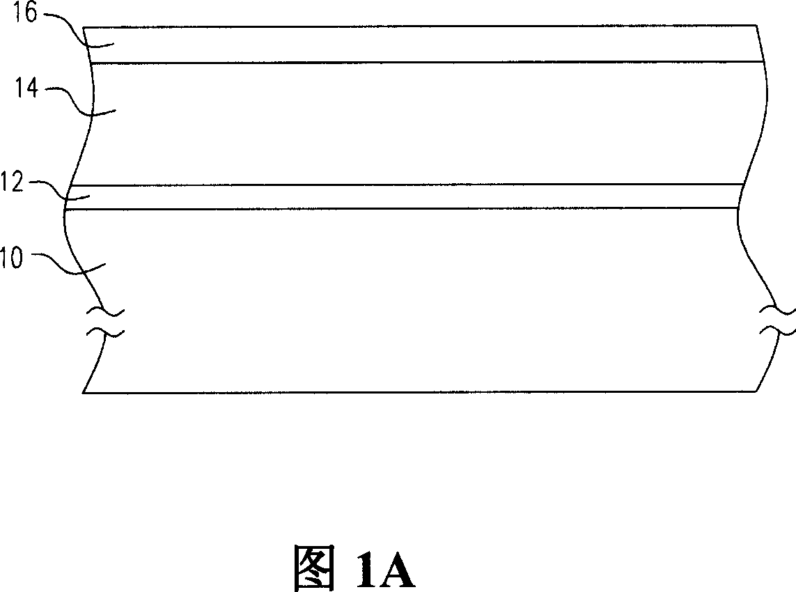
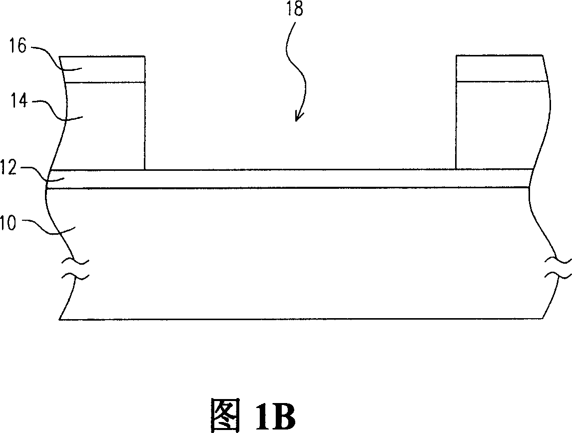
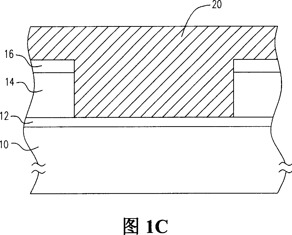
[0035] 1A to 1H are partial cross-sectional schematic diagrams of the manufacturing process of a field emission triode element of the present invention. Please refer to FIG. 1A. First, a cathode conductive layer 12, an insulating layer 14 and a gate layer 16 are sequentially formed on a substrate 10. . The substrate 10 is, for example, a silicon substrate or a glass substrate. The cathode conductive layer 12 is a cold cathode conductive material used as a field emission triode element, and its material is, for example, single-layer or double-layer metal, alloy, metal nitride or doped semiconductor. The cathode conductive layer 12 can also provide good adhesion between the substrate 10 and the insulating layer 14 , and its thickness is about 0.05 μm to 0.5 μm. In a preferred embodiment, the material of the cathode conductive layer 12 is, for example, titanium, titanium nitride, tantalum or tantalum nitride. The above materials can withstand a process temperature above 800° C.,...


PUM

PropertyMeasurementUnit
thicknessaaaaaaaaaa
thicknessaaaaaaaaaa
diameteraaaaaaaaaa

Abstract

This inventing relates to triode element process method, which comprises the following steps: forming cathode conductor layer, insulation layer and grating layer on base and forms explosion part cathode conductive layer on grating layer and insulation layer; then forming metal layer on cathode layer for first anode process to form first anode process layer; then removing first anode process layer then to form second anode process layer with multiple holes; then forming catalyze layer on hole bottom and then forms multiple nanometer tube in holes.

Description

technical field [0001] The invention relates to a manufacturing method of a field emission triode element, in particular to a manufacturing method of a carbon nanometer carbon tube field emission triode element. Background technique [0002] Field emission display (Field Emission Display, FED) has been paid more and more attention due to its advantages of high brightness, wide viewing angle, and rapid instantaneous response. It is a better field emission cathode (cathode emitter) material for a flat panel display. [0003] In the known carbon nanotube field emission device manufacturing technologies, most of them use chemical vapor deposition to directly grow carbon nanotubes on the cathode area where the metal catalyst is distributed. However, the carbon nanotubes grown by this method will show a disordered distribution in the cathode region. Under general field emission operating conditions, the number of carbon nanotubes that can be aligned parallel to the electric field...

Claims


Application Information

Patent Timeline
Patent Type & Authority Applications(China)
IPC IPC(8): H01J9/02H01J31/12H01L21/00
Inventor 潘扶民陈柏林林贞君刘梅莫启能
Owner CHUNGHWA PICTURE TUBES LTD
Learn More