Method for manufacturing flexible circuit board

A technology of flexible circuit boards and manufacturing methods, which is applied in the fields of printed circuit manufacturing, printed circuits, printed circuits, etc. It can solve the problems of low line fineness, difficulty in attaching intact, unstable lines and hole yields, etc., and achieve glass light transmission Good resistance, not easy to be deformed by heat, and the effect of improving production yield

Inactive Publication Date: 2007-03-28
AVARY HLDG (SHENZHEN) CO LTD +1
View PDF0 Cites 8 Cited by
  • Summary
  • Abstract
  • Description
  • Claims
  • Application Information

AI Technical Summary

Problems solved by technology

[0024] The manufacturing process of the above method has the following defects: First, the manufacturing process uses dry film etching, which needs to be coated with photoresist on the entire surface, and then exposed and developed. The purpose of coating the entire surface is to protect the parts that do not need to be etched from being etched
However, because air bubbles will be generated when the dry film is pressed, the adhesion is poor. During the production process, the sprocket hole is driven by the sprocket to realize continuous operation. Therefore, the dry film around the sprocket hole is easy to fall off due to the movement of the sprocket. It is difficult to adhere well. In the subsequent production process, after exposure, development, and etching, the copper and substrate around the sprocket hole without dry film protection will also be etched away, resulting in the sprocket hole being easily broken
Secondly, the sprocket holes play a positioning role in the process of making holes and circuits. After the above etching, the positioning is not accurate, making the yield of circuits and holes unstable.
Thirdly, using dry film etching technology, due to the thick dry film thickness and poor adhesion, the fineness of the formed circuit is low
Finally, this method uses a plastic photomask during exposure and development. The plastic photomask is easily deformed by heat, and the required line width cannot be achieved during image transfer, resulting in a decrease in yield.

Method used


Image

  • Method for manufacturing flexible circuit board
  • Method for manufacturing flexible circuit board
  • Method for manufacturing flexible circuit board

Examples


Embodiment Construction

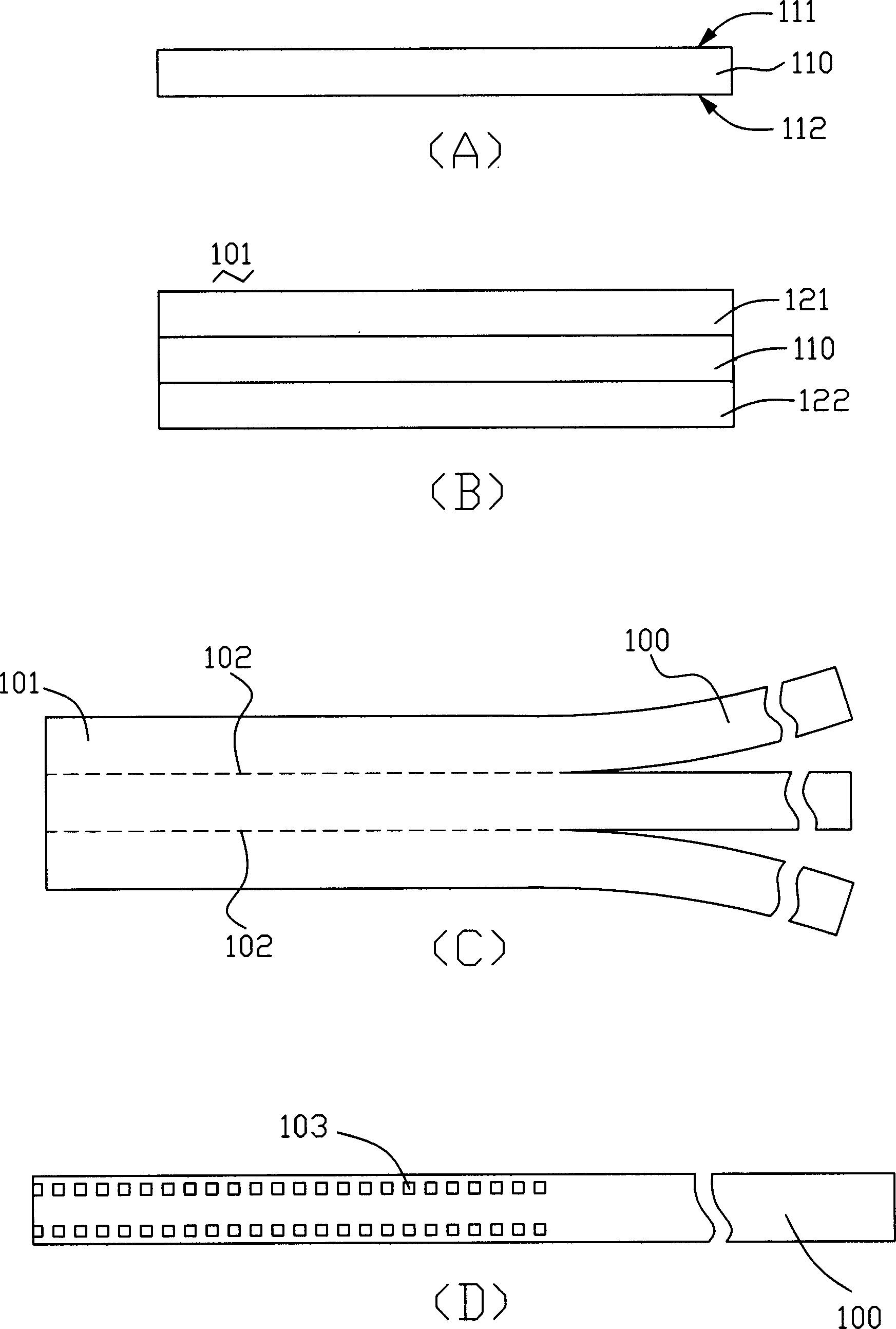
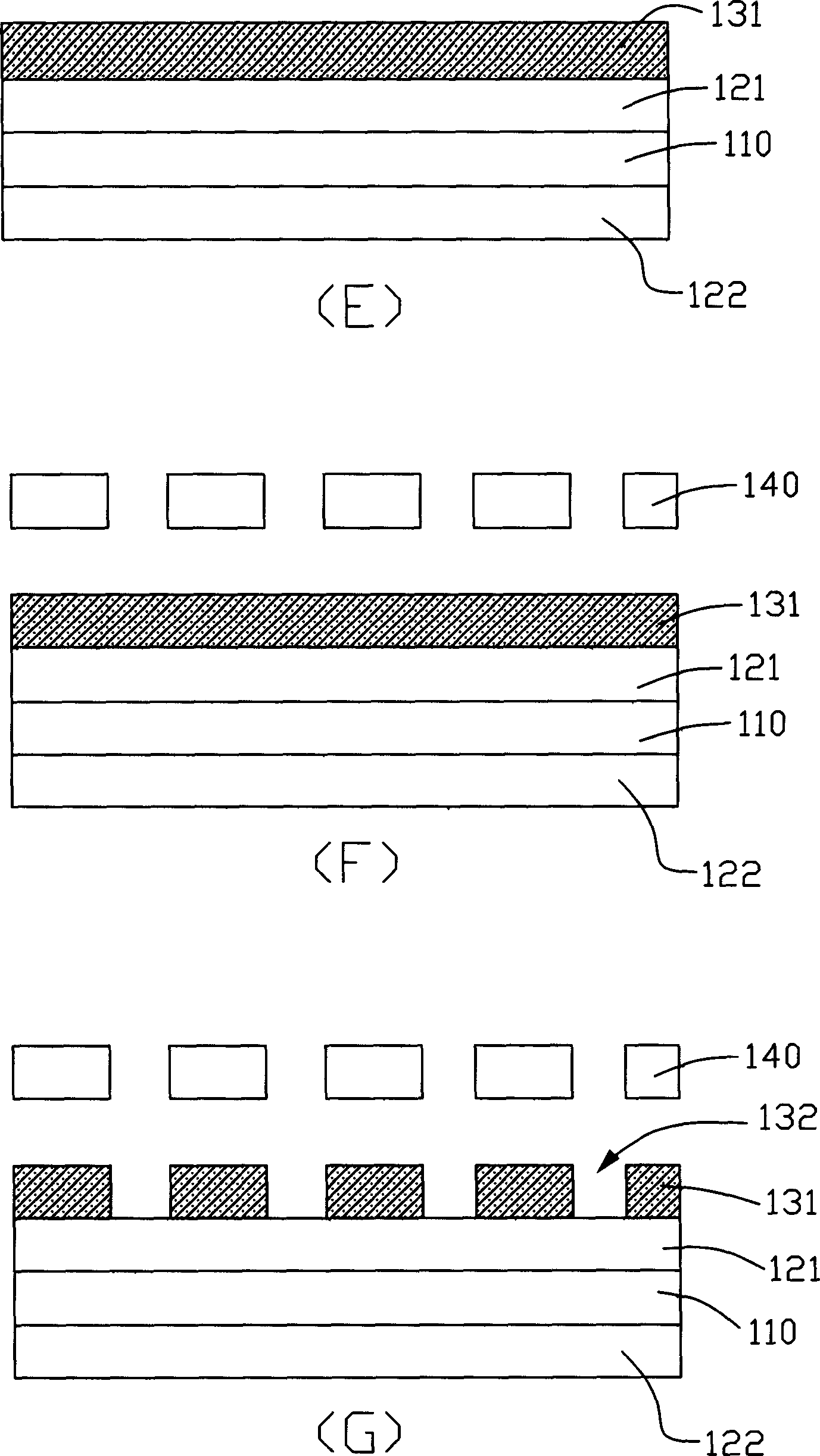
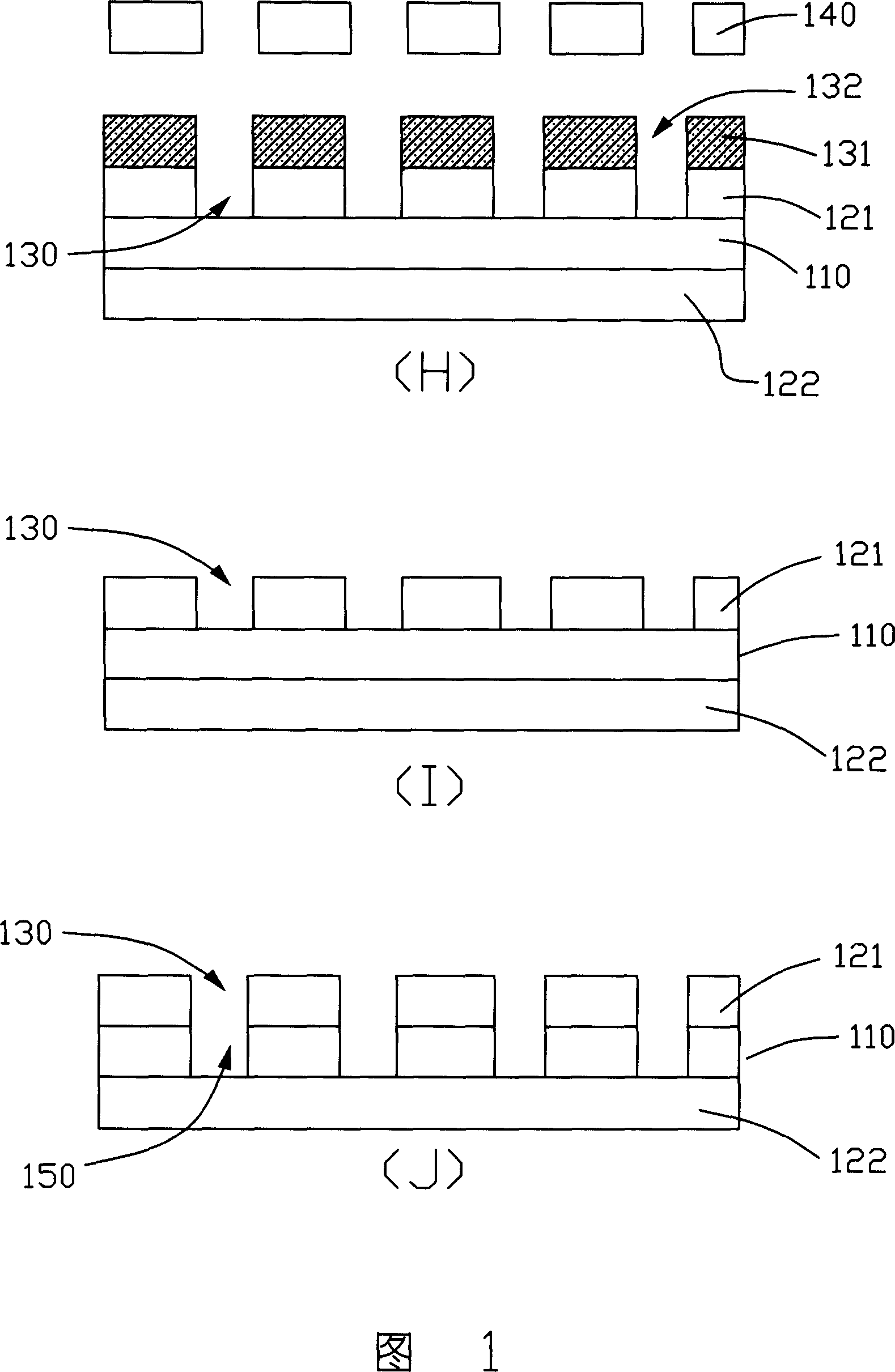
[0036] The flexible circuit board of this embodiment is made of a substrate with a copper film on at least one surface through complicated operations. It has a plurality of holes and circuits on the surface of the substrate. The holes are generally made of copper formed on the copper film. Pores and film pores formed in the substrate. Wherein the material of the substrate can be polyimide, polyester, Teflon, polymethyl methacrylate or carbonate and the like.

[0037] Please refer to FIG. 2 and FIG. 3 together, which are schematic diagrams of the manufacturing process and method of the flexible circuit board in this embodiment. This embodiment comprises the steps:

[0038] (1) As shown in Fig. 3 (A), at first provide a substrate 210, it has a first surface 211 and an opposite second surface 212, and its material is polyimide, also can be polyester etc.;

[0039] (2) As shown in Fig. 3 (B) (being cross-sectional view), form a first copper film 221 on this first surface 211, fo...


PUM


Abstract

The invention supplies a kind of method of creating the flexible circuit board. The step is as follows. The treated component has the base on which there is at least one copper film. Multiple copper holes form on the copper film. The copper holes form by micro-image process that includes the step of coating photoresist layer. The photoresist material is liquid. The micro-image process also includes the steps of exposal, developing, etching and peeling film. The light cover in the step of exposal is vitric.

Description

【Technical field】 [0001] The invention relates to a method for manufacturing a flexible circuit board, in particular to a method for manufacturing a flexible circuit board that can improve the rigidity of a sprocket hole, have high line precision and stable yield. 【Background technique】 [0002] With the continuous development of science and technology, ultra-small mobile phones, portable calculators and automotive electronic products have put forward higher requirements for the miniaturization and light weight of products. In order to meet this demand, the integration degree of circuits in electronic products has been continuously improved, the pattern of printed circuits has become increasingly dense, and the conductor width, conductor spacing, and through-hole size of the circuit have also become increasingly smaller. Therefore, flexible printed circuit boards (Flexible Printed Circuit, abbreviated FPC, also known as soft boards, flexible circuit boards or flexible circui...

Claims


Application Information

Patent Timeline
Patent Type & Authority Applications(China)
IPC IPC(8): H05K3/06H05K3/42H05K1/09H05K1/00
CPCH05K1/0393H05K3/421H05K3/064H05K2201/09509H05K2203/0554H05K2203/0759H05K3/002H05K2201/0394H05K3/427
Inventor 廖家骏江伯彦
Owner AVARY HLDG (SHENZHEN) CO LTD
Why Eureka
Try Eureka