Dry cleaning system using a laser

A purification system and laser technology, applied in the field of dry purification systems using lasers, can solve problems such as environmental pollution and discharge of sewage and waste water, and achieve the effect of simple cleaning automation process, improving test efficiency, and saving production costs.

Inactive Publication Date: 2007-04-04
IMT INC
View PDF0 Cites 21 Cited by
  • Summary
  • Abstract
  • Description
  • Claims
  • Application Information

AI Technical Summary

Problems solved by technology

Furthermore, the use of chemical wet purification methods will discharge a large amount of sewage and

Method used


Image

  • Dry cleaning system using a laser
  • Dry cleaning system using a laser
  • Dry cleaning system using a laser

Examples


Embodiment Construction

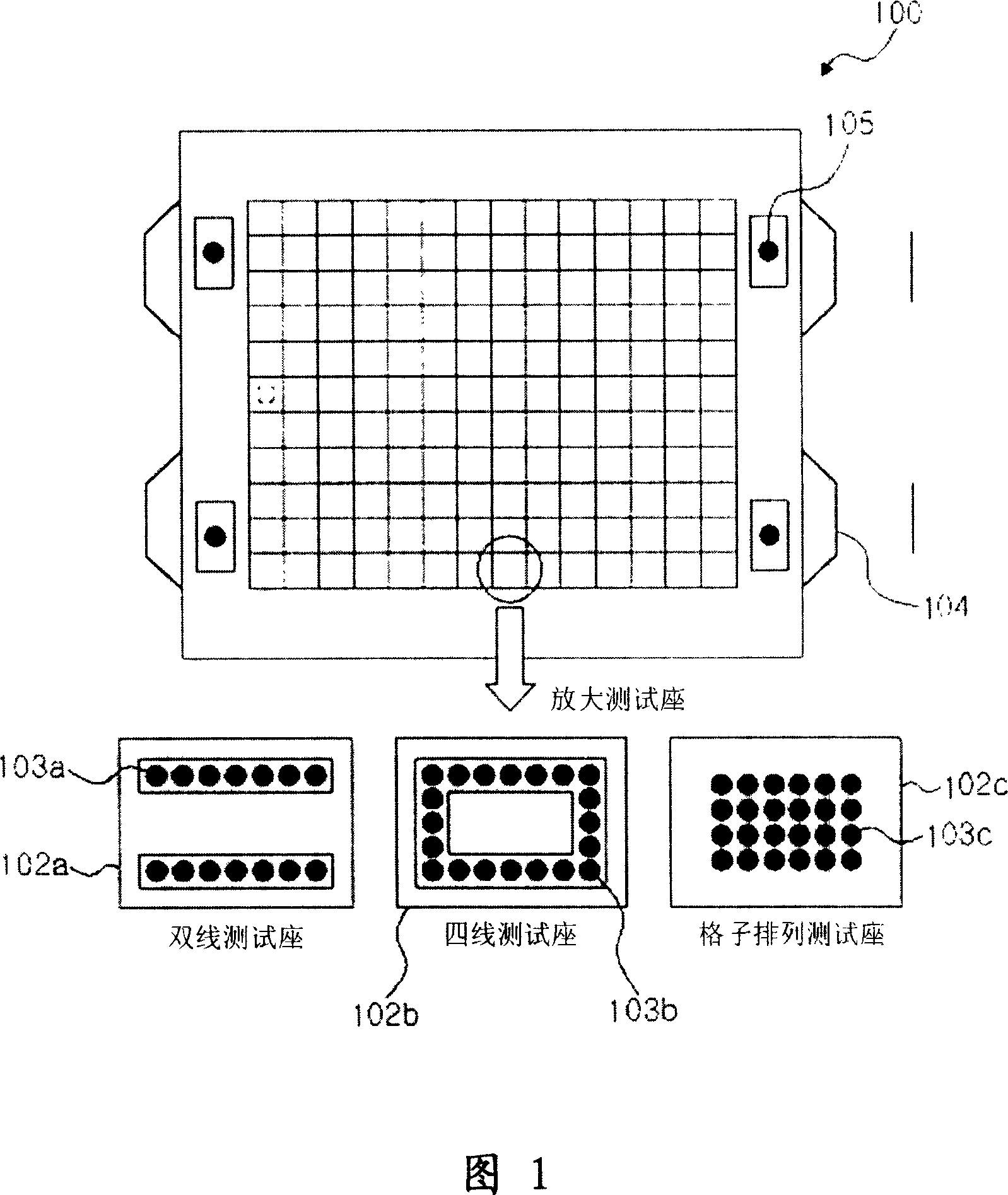
[0048] Below, the preferred embodiment of the present invention will be described in detail with reference to the accompanying drawings. In the accompanying drawings of the following embodiments, the objects to be cleaned include but are not limited to the semiconductor test seat board and the test seat contact portion thereon, and probe cards for wafer testing, etc. can also be used as cleaning objects.

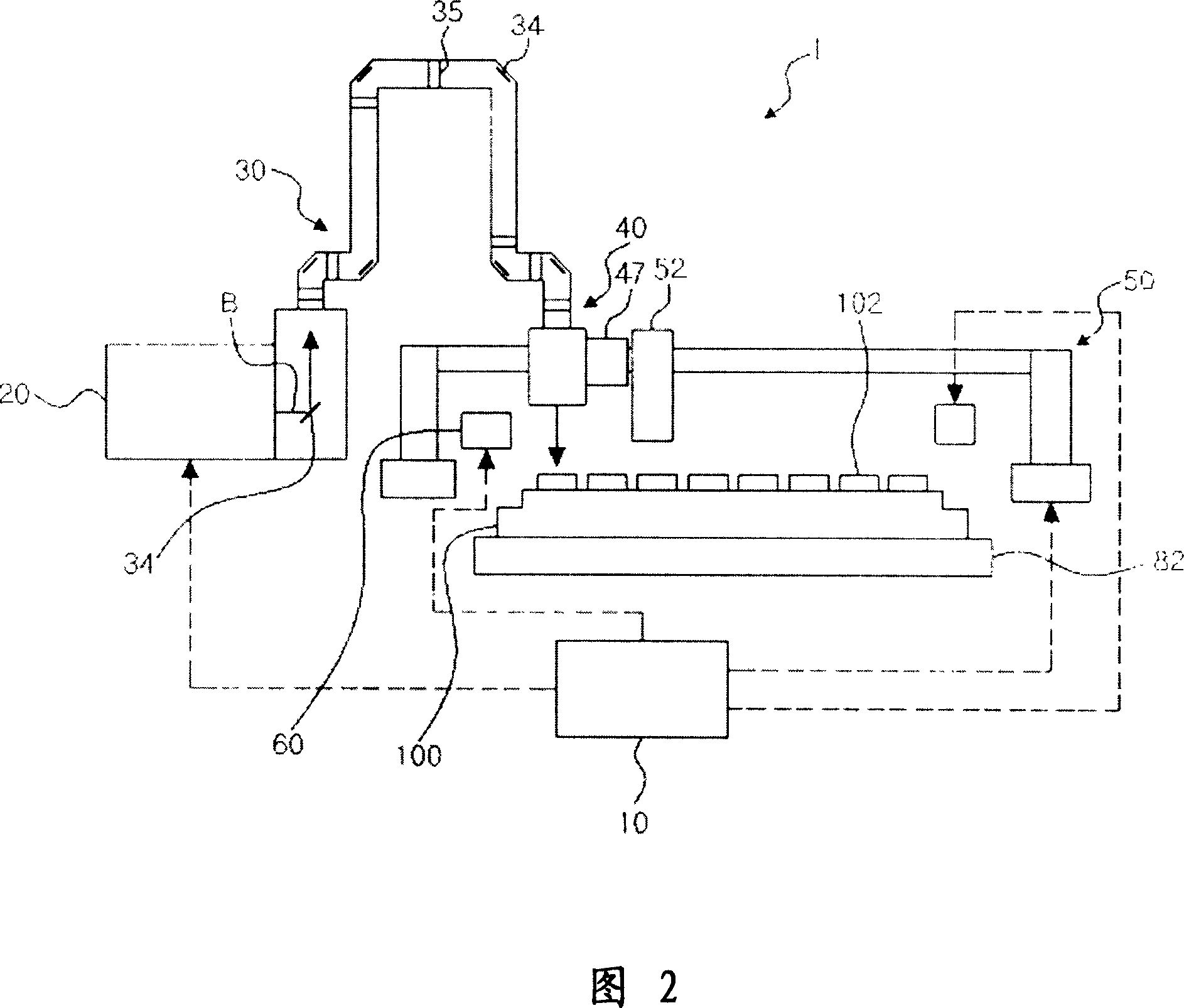
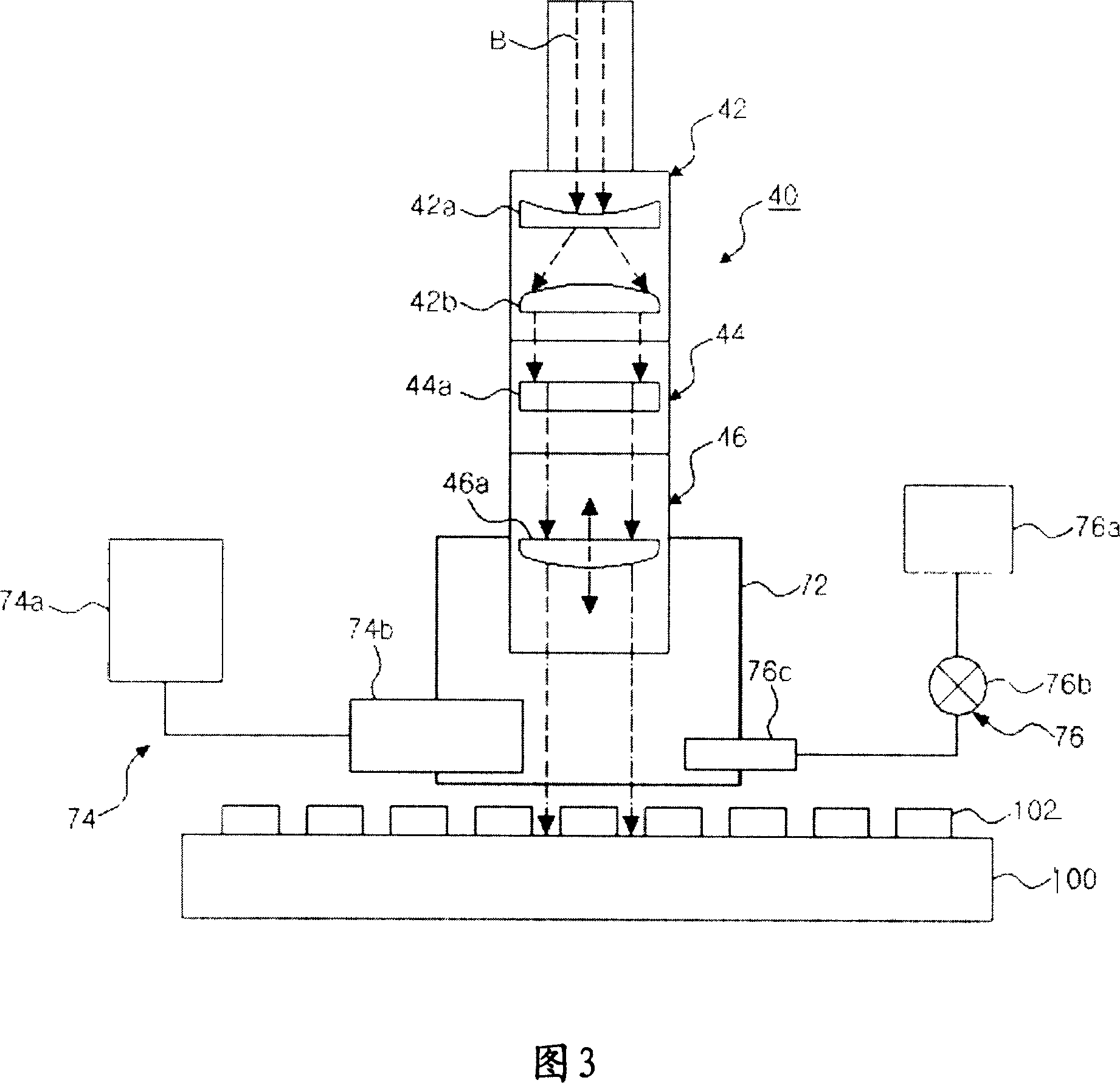
[0049] Please refer to FIG. 2 , which is a schematic diagram of a dry cleaning system for dry-cleaning semiconductor test sockets in an embodiment of the present invention. Fig. 3 illustrates the main parts of the dry cleaning system in Fig. 2, and is a schematic diagram of a laser beam irradiation device for irradiating objects to be cleaned with laser beams. Fig. 4 is a schematic diagram of a carrying device for loading the cleaning object-semiconductor test board into the dry system.

[0050] Please refer to FIG. 2 , the dry purification system 1 of this embodiment inclu...


PUM

PropertyMeasurementUnit
Wavelengthaaaaaaaaaa

Abstract

The present invention relates to a dry cleaning system for removing the contamination from the cleaning object using a laser, and is directed to provide a dry cleaning system capable of removing contamination from the cleaning object effectively by using optical energy-laser, particularly removing contamination from the surface of the contact part of Semiconductor Test socket. According to the present invention, the dry cleaning system using laser is composed of: a laser generator for generating laser beam; a laser beam transmitting device for transmitting the laser beam generated from the laser generator; a laser beam irradiation device for adjusting the form of the laser beam transmitted by the laser beam transmitting device and irradiating the adjusted laser beam to the cleaning object; a scanning device for adjusting the irradiation position of the laser beam from the laser beam irradiation device.

Description

technical field [0001] The present invention relates to a dry cleaning system utilizing laser light and a cleaning method thereof, and in particular to having an appropriate structure for removing contamination from the surface contact portion of a semiconductor test seat board or the surface of a probe card for wafer testing Dry purification system for pollutants. Background technique [0002] Semiconductor testing is an electrical test process to judge the quality of each semiconductor device manufactured through assembly process. In order to test a large number of semiconductor devices at once, we use a test socket board whose surface is provided with a large number of test sockets to test each device individually. [0003] Please refer to FIG. 1 , which illustrates a commonly used test seat board 100 for electrical testing of semiconductor devices. The size (length and width) of the test seat board 100 is more than 500×500 mm, and it can be divided into two types accor...

Claims


Application Information

Patent Timeline
IPC IPC(8): B23K26/36B23K26/08B23K26/42B23K26/18B23K26/16B23K26/04B23K26/06B08B7/00B23K26/00H01L21/268
CPCB23K26/352H01L21/268H01L21/3065
Inventor 李锺明
Owner IMT INC
Why Eureka
Try Eureka