Method for making vertical double diffusion FET compatible conventional FET

A vertical double-diffusion, FET technology, used in semiconductor/solid-state device manufacturing, electrical components, circuits, etc., can solve the problem that the control chip has a reduced ability to monitor overheating of the output chip, increased circuit reliability, and increased packaging costs. and other problems, to achieve the effect of solving reliability degradation, realizing high voltage and high current control, and low power consumption

Active Publication Date: 2007-04-18
无锡市晶源微电子股份有限公司
View PDF0 Cites 18 Cited by
  • Summary
  • Abstract
  • Description
  • Claims
  • Application Information

AI Technical Summary

Problems solved by technology

In this way, the technical difficulty is reduced, but the cost of packaging is greatly increased
At the same time, the use of dual chips increases the power consumption; due to the different islands, the c

Method used


Image

  • Method for making vertical double diffusion FET compatible conventional FET
  • Method for making vertical double diffusion FET compatible conventional FET
  • Method for making vertical double diffusion FET compatible conventional FET

Examples


Embodiment Construction

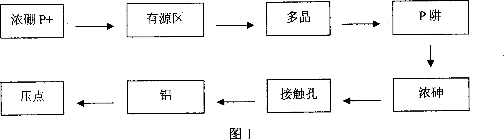
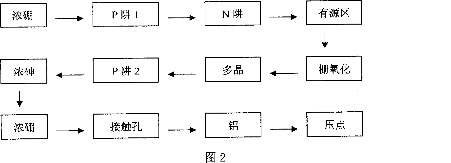
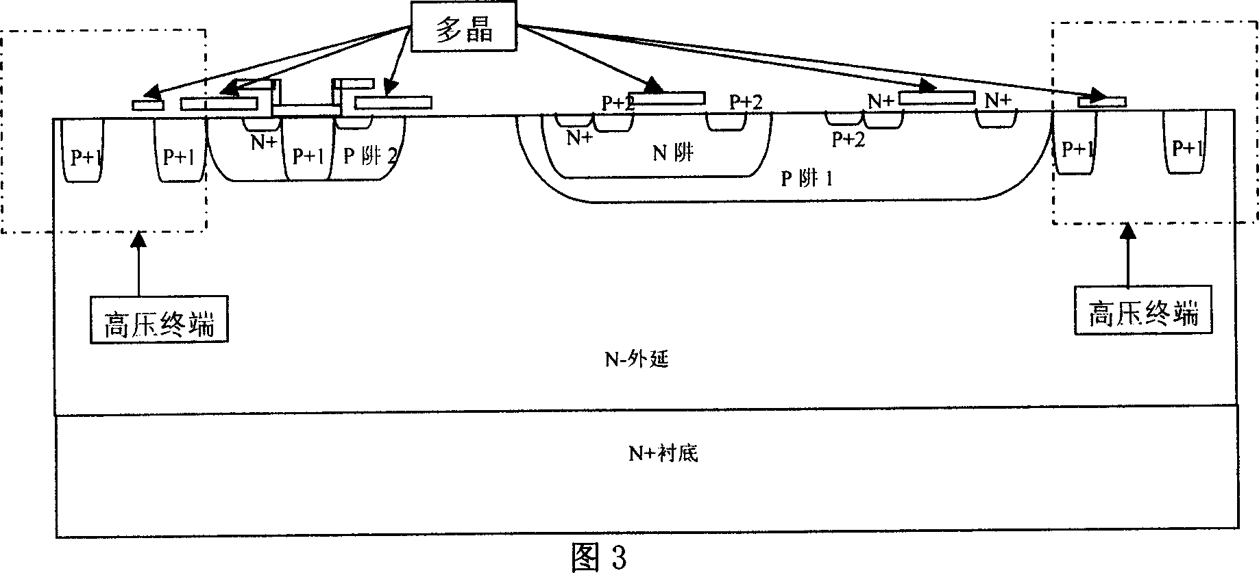
[0037] Under this platform, we realized the integration of control circuit and output high voltage VDMOS on the chip area of ​​2000*2200μm. The specific implementation is as follows:

[0038] 1.) High-concentration P+ implantation, pushing junction depth: The concentration and junction depth here have a great impact on the withstand voltage of the entire die. The specific concentration and junction depth should be adjusted appropriately according to the corresponding layout design.

[0039] 2.) Inject PWELL1 in the low-pressure area, and pre-push the junction depth: here is only a pre-push junction depth, and the junction depth should not be pushed too deep. Because there are still many high-temperature processes behind, the junction will be further deepened.

[0040] 3.) NWELL implantation in low-voltage area, pre-push junction depth: PWELL and NWELL for low-voltage CMOS are added before ACTIVE (active area). The junction depth of PWELL and NWELL here should not be pushed ...


PUM


Abstract

The invention is a vertical bilateral diffusion field-effect transistor (FET) compatible routine FET making method, a BCD process method for making high voltage integrated circuits, adopting silicon slice to make VDMOS, making high concentration P+1 injection in the periphery of a chip and extending junction depth; making PWELL1 injection in low voltage region, making NWELL injection in low voltage region, preoxidizing grid of the whole chip, injecting P impurity into the whole slice and oxidizing, etching thick oxide layer, then oxidizing the whole slice, depositing, doping and etching on the whole polycrystalline silicon slice, after etching, retaining voltage dividing field plate, making PWELL2 B injection in VDMOS region, and extending junction depth; making N+ As injection in a region used to make VDMOS source, and NMOS source/drain and PMOS substrate bias of CMOS, substrate bias of PMOS, and making B injction 'P+2' in the positions of PMOS source/drain and NMOS substrate bias of CMOS, making contact hole etching, evaporating aluminum on the whole chip, corroding aluminum to form meal leads, and etching pressure point.

Description

technical field [0001] The invention relates to a BCD (Bipolar / CMOS / DMOS) process method for manufacturing HVIC (High Voltage Integrated Circuit), which belongs to the technical field of semiconductor manufacturing. Background technique [0002] With the continuous development of semiconductor technology, HVIC is widely used. The continuous development of semiconductor process technology. BIPOLAR (bipolar), CMOS (complementary metal-oxide-semiconductor field-effect transistor) and DMOS (double-diffused metal-oxide-semiconductor field-effect transistor) have been continuously integrated with each other, and gradually developed the integration of BIPOLAR and CMOS The BICMOS and the BCD process integrated by the three. The integrated BCD process of Bipolar / CMOS / DMOS is used to combine three different process types: bipolar is for analog control; CMOS is for digital control; DMOS is for processing high voltage and high current in chip or system management. Realize the soft st...

Claims


Application Information

Patent Timeline
IPC IPC(8): H01L21/8238
Inventor 朱伟民聂卫东易法友郭斌张艳丽
Owner 无锡市晶源微电子股份有限公司
Why Eureka
Try Eureka