Homojunction combined gate field effect transistor

A technology of field-effect transistors and compound gates, which is applied in semiconductor devices, electrical components, circuits, etc., can solve the problems of small-sized MOSFETs, high-work function materials, and difficult realization, so as to suppress short-channel effects, The effect of adjusting the threshold voltage and increasing the driving current

Inactive Publication Date: 2007-04-25
ANHUI UNIVERSITY
View PDF0 Cites 6 Cited by
  • Summary
  • Abstract
  • Description
  • Claims
  • Application Information

AI Technical Summary

Problems solved by technology

From the perspective of gate engineering, it is mainly a method of changing the gate material and gate structure, such as a heterogeneous gate MOSFET. Although the structure obtained in this way increases the movement speed of carriers, it leads to an increase in the cut-off frequency and maximum operating frequency of the MOSFET. , but because high work function materials are difficult to realize by technology, it is difficult to be used in small-size MOSFET process practice at present
From the perspective of channel engineering, it is to change the doping distribution of the channel. The typical halo structure is characterized by reducing the field strength of the drain terminal to reduce the DIBL effect and hot electron injection effect, and to improve the electrical characteristics and reliability of the device. characteristics, but the process is complicated, and it is difficult to implement in small-size MOSFETs

Method used


Image

  • Homojunction combined gate field effect transistor
  • Homojunction combined gate field effect transistor

Examples


Embodiment 1

[0036] In embodiment 1, the channel length is set to 0.35um, and other related settings include:

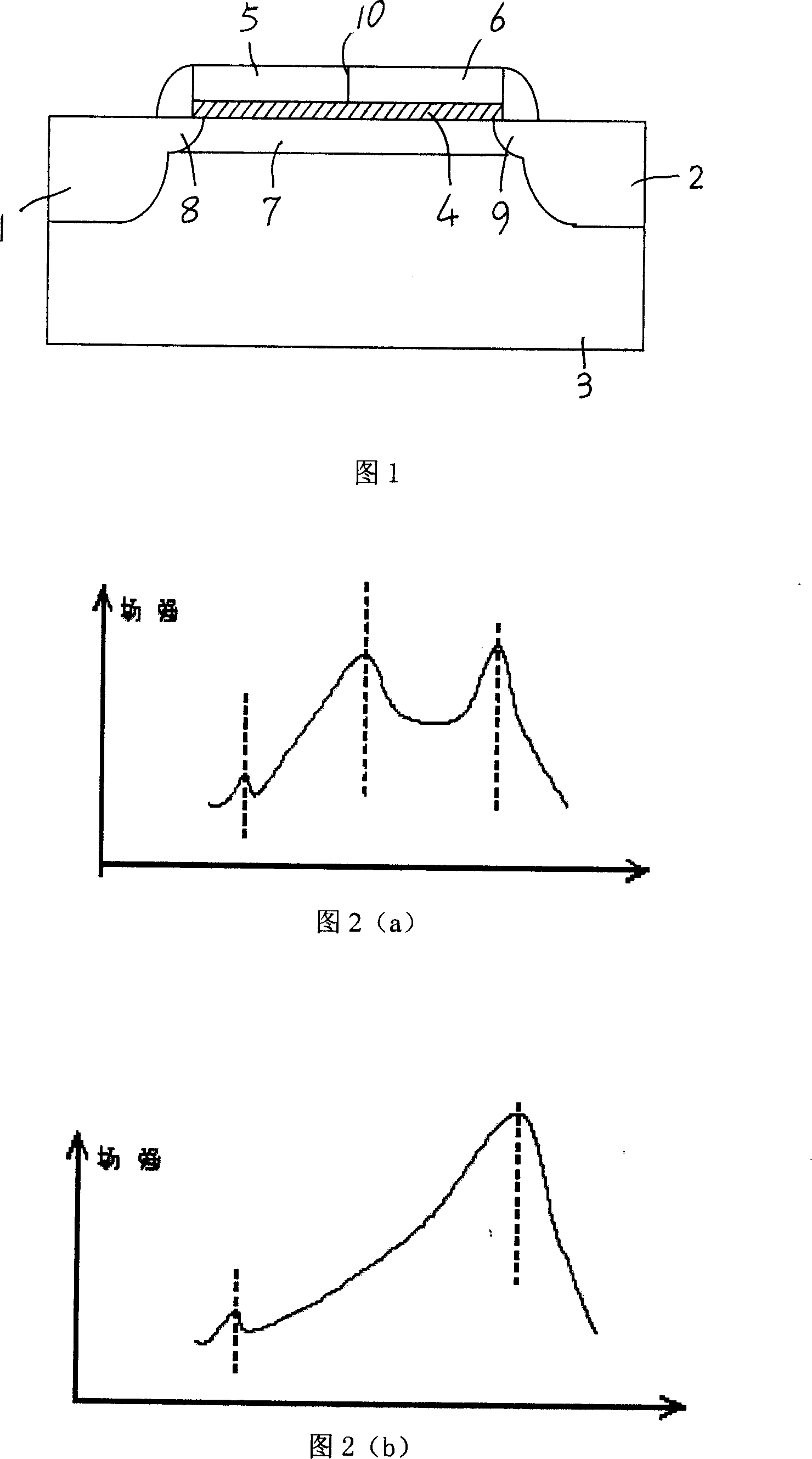
[0037] The thickness of the insulating layer 4 is 7nm, and the doping concentrations of the source terminal 1 and the drain terminal 2 are both 1×10 20 cm -3 , the junction depth is 150nm; the doping concentration of shallow source extension region 8 and shallow drain extension region 9 is 1×10 20 cm -3 , the junction depth is 50nm, and the doping concentration of the substrate 3 is 3×10 17 cm -3 . The doping concentration of the P-type polysilicon gate 5 at the gate end is 1×10 20 cm -3 , the doping effect is P + And the doping concentration of the N-type polysilicon gate 6 is 1×10 20 cm -3 , the doping effect is N + , and the length ratio between them is 1:1.

Embodiment 2

[0038] Example 2: Set the channel length to 0.25um, other related settings include:

[0039] The thickness of the insulating layer 4 is 5nm, and the doping concentrations of the source terminal 1 and the drain terminal 2 are both 1×10 20 cm -3 , the junction depth is 150nm; the doping concentration of shallow source extension region 8 and shallow drain extension region 9 is 1×10 19 cm -3 , the junction depth is 50nm, and the doping concentration of the substrate 3 is 3×10 16 cm -3 . The doping concentration of the P-type polysilicon gate 5 at the gate end is 1×10 20 cm -3 , the doping effect is P + And the doping concentration of the N-type polysilicon gate 6 is 1×10 20 cm -3 , the doping effect is N + , and the length ratio between them is 1:1.

Embodiment 3

[0040] Example 3: Set the channel length to 0.13um, and other related settings include:

[0041] The thickness of the insulating layer 4 is 2nm, and the doping concentrations of the source terminal 1 and the drain terminal 2 are both 1×10 20 cm -3 , the junction depth is 150nm; the doping concentration of shallow source extension region 8 and shallow drain extension region 9 is 1×10 20 cm -3 , the junction depth is 50nm, and the doping concentration of the substrate 3 is 3×10 17 cm -3 . The doping concentration of the P-type polysilicon gate 5 at the gate end is 1×10 20 cm -3 , the doping effect is P + And the doping concentration of the N-type polysilicon gate 6 is 1×10 20cm -3 , the doping effect is N + , and the length ratio between them is 1:1.

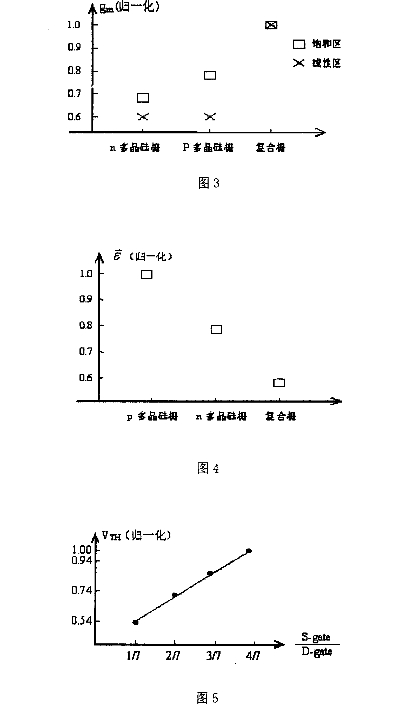
[0042] The characteristics of the device were simulated by the two-dimensional device simulation software - MEDICI, and the conclusions are as follows:

[0043] Table 1. Electrical characteristics of three gate electro...


PUM


Abstract

The invention relates to a composite grid field effect transistor. Wherein, the grid, source, leak and substrate form the main body; the insulated layer is between grid and substrate; the groove is on the substrate between source and leak; the source extends shallow source extending area at the left end of groove; the grid extends shallow leak extending area at the right end; the invention is characterized in that the grid is composite grid and multi-crystal grid, while the left and right parts are different in conductive types; the left grid toward to source is P-type multi-crystal grid, while the left part toward leak is N-type multi-crystal grid. The invention can obtain radio MOSFET driving current, transconductance and cut-off frequency, and release the maximum field strength, thermal electronic effect and short-groove effect at the end of leak drift area.

Description

[0001] Technical field [0002] The invention belongs to the technical field of microelectronics and semiconductors, in particular to a homogeneous composite gate field effect transistor. Background technique [0003] With the development of communication technology, radio frequency integrated circuits are used more and more widely, and the operating frequency of the circuit is also rapidly increasing. It is expected that when the 3G era comes in the near future, the radio frequency used in communication will increase from 900MHZ to 1.885-2.025GHZ, so it is used for The cut-off frequency and maximum operating frequency of MOSFETs in radio frequency integrated circuits will also be greatly improved. From the perspective of semiconductor device physics, improving the high frequency characteristics of MOSFET is nothing more than two methods of gate engineering and channel engineering. From the perspective of gate engineering, it is mainly a method of changing the gate material a...

Claims


Application Information

Patent Timeline
Patent Type & Authority Applications(China)
IPC IPC(8): H01L29/772H01L29/78H01L29/808H01L29/49
Inventor 陈军宁柯导明徐超代月花高珊孟坚吴秀龙
Owner ANHUI UNIVERSITY
Why Eureka
Try Eureka