

Process for preparing multiple ATO nanometer structure
A nanostructure and ATO technology, applied in the direction of tin oxide, etc., can solve the problems of ATO nano-products with single shape, complex process, high production cost, etc., and achieve the effect of low requirements on reaction conditions, simple process flow and single raw material
- Summary
- Abstract
- Description
- Claims
- Application Information
AI Technical Summary
Problems solved by technology
Method used
Image

Examples
Embodiment 1
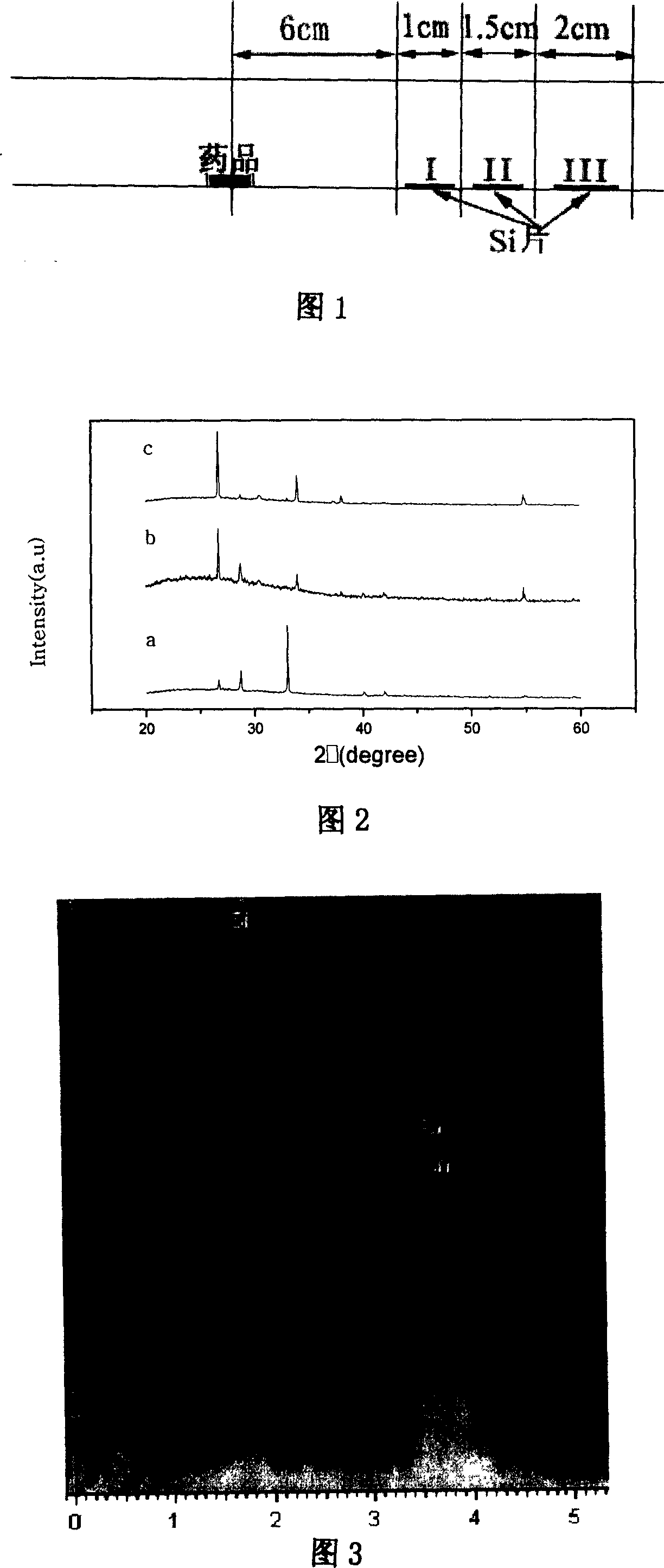
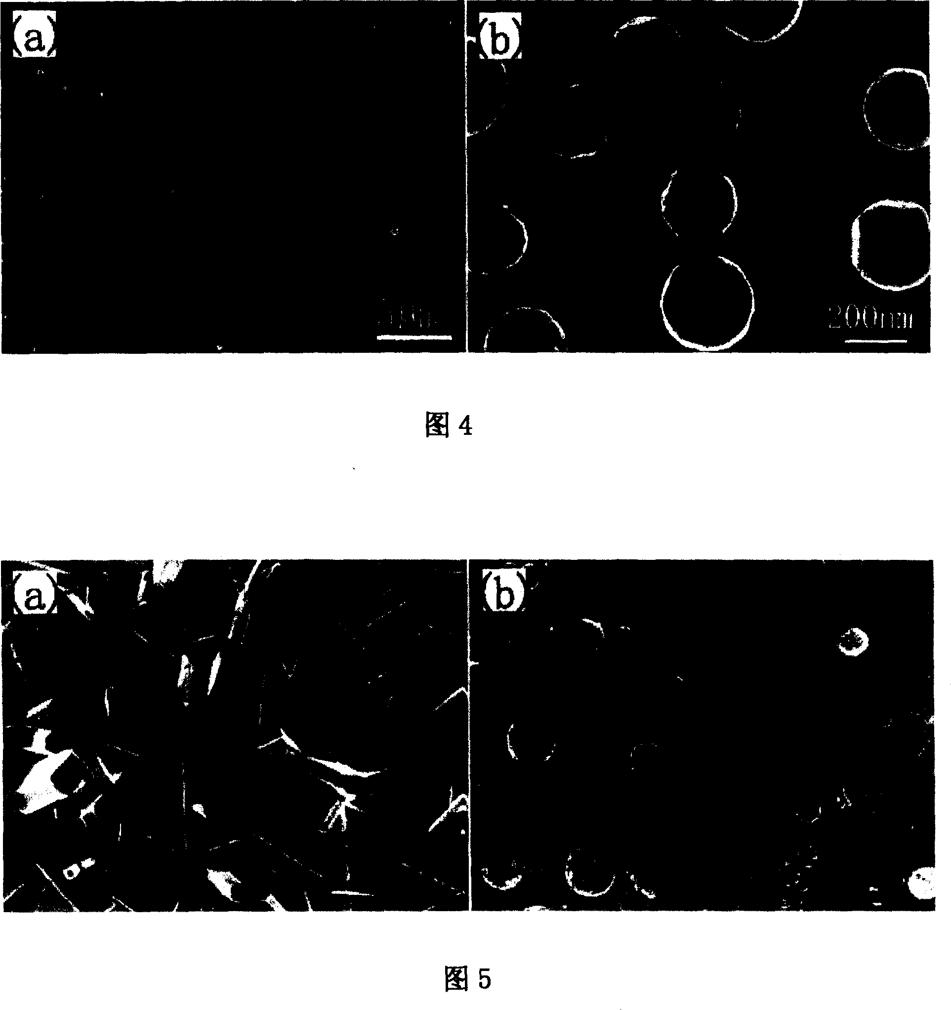
[0050] Place a ceramic boat containing 3 g of mixed powder (the mass ratio of graphite to ATO is 1:6) in the middle of the ceramic tube, and three silicon chips are placed in another ceramic boat and placed downstream of the carrier gas in the ceramic tube, as shown in Figure 1 . Before heating, flow argon gas with a flow rate of 100 sccm into the system from one end of the ceramic tube for about 1 hour to remove the air in the ceramic tube, then set the reaction temperature to 1150°C, the reaction time is 1.5 hours, and the argon gas flow rate during heating is 50 sccm. After the reaction was completed, the system was naturally cooled to room temperature and the products obtained on three silicon wafers were collected. Observation with a scanning electron microscope revealed that the morphology of the products in different deposition areas was different. The product in region I in Fig. 1 is a solid nanosphere, as shown in Fig. 4 . Region II is nanorods, as shown in Fig. 5(a)...
Embodiment 2
[0052] A ceramic boat containing 3 g of mixed powder (the mass ratio of graphite to ATO is 1:6) was placed in the middle of the ceramic tube, and the ceramic boat filled with silicon wafers was placed about 10 cm away from the medicine. After heating, put argon gas with a flow rate of 100 sccm into the system for about 1 hour to remove the air in the tube, then set the reaction temperature to 1000 ° C, the reaction time is 1.0 h, and the argon gas flow rate is 30 sccm during heating. After the reaction is over, the system is naturally cooled to room temperature The product obtained on the silicon wafer was collected, its morphology was observed by field emission scanning electron microscope (FESEM), and its composition and content were investigated by X-ray diffraction (XRD) and energy spectrum (EDS). The deposits on the silicon wafer were found to be nano-solid spheres by scanning electron microscope observation, as shown in FIG. 4 .
Embodiment 3
[0054] A ceramic boat containing 3 g of mixed powder (the mass ratio of activated carbon to ATO is 1:3) was placed in the middle of the ceramic tube, and the ceramic boat filled with silicon wafers was placed about 10 cm away from the medicine. After heating, let the argon gas with a flow rate of 100 sccm into the system for about 1 hour to remove the air in the tube, then set the reaction temperature to 1050°C, the reaction time is 2.0 hours, and the argon gas flow rate is 50 sccm during heating. After the reaction is over, the system is naturally cooled to room temperature The obtained product was collected, its morphology was observed by field emission scanning electron microscope (FESEM), and its composition and content were investigated by X-ray diffraction (XRD) and energy spectrum (EDS). The deposits on the silicon wafer were found to be nanorods by scanning electron microscope observation, as shown in Figure 5(a).
PUM
 Abstract
Description
Claims
Application Information