Array base plate of thin film transistor of LCD and manufacturing method of the same
A technology of thin-film transistors and liquid crystal displays, which is applied in semiconductor/solid-state device manufacturing, instruments, exposure devices for photolithography, etc., and can solve problems such as high production costs
- Summary
- Abstract
- Description
- Claims
- Application Information
AI Technical Summary
Problems solved by technology
Method used
Image

Examples
Embodiment 1
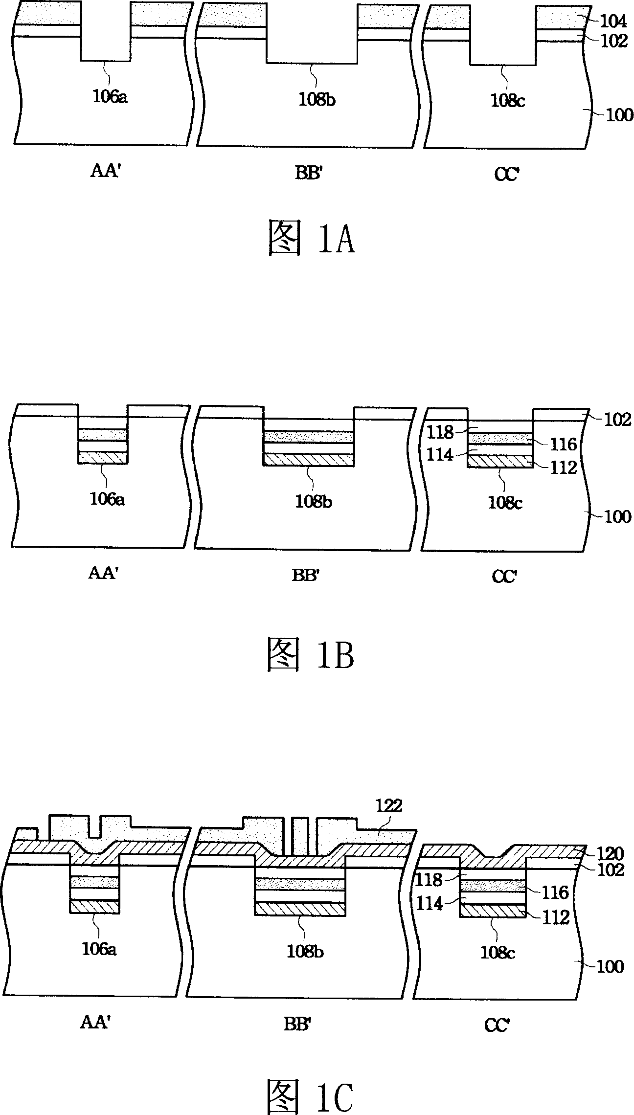
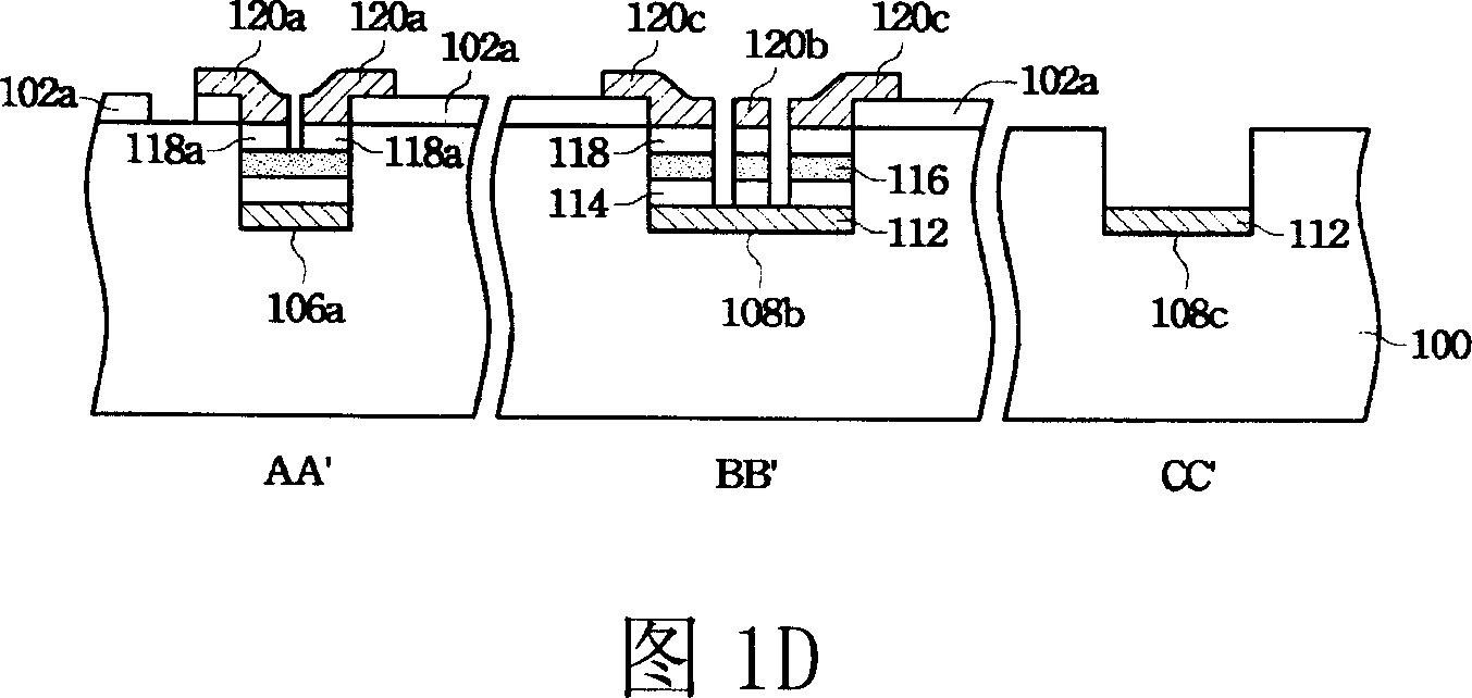
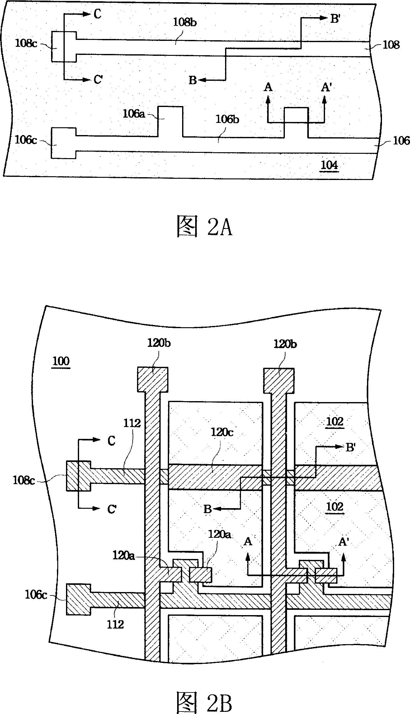
[0040] 1A-1D are schematic cross-sectional structural diagrams of the manufacturing process of a thin film transistor array substrate of a liquid crystal display according to an embodiment of the present invention, and FIGS. 2A-2B are schematic top views of the thin film transistor array substrate of a liquid crystal display at different manufacturing stages.
[0041] Please refer to FIG. 1A and FIG. 2A at the same time. FIG. 2A is a schematic top view of FIG. 1A . A transparent conductive layer 102 and a first photoresist layer 104 are sequentially formed on the substrate 100, and then the first photomask is used to perform a photolithographic etching process, and the scanning line channel 106 and the capacitance line channel are simultaneously formed on the substrate 100. Road 108. The substrate 100 other than the scan line channel 106 and the capacitor line channel 108 is still covered by the transparent conductive layer 102 and the first photoresist layer 104 in sequence. ...
Embodiment 2
[0053] 3A-3G are schematic cross-sectional structural diagrams of the manufacturing process of a thin-film transistor array substrate of a liquid crystal display according to an embodiment of the present invention, and FIGS. 4A-4B are schematic top views of the thin-film transistor array substrate of a liquid crystal display at different manufacturing stages.
[0054] In FIG. 3A , firstly, a transparent conductive layer 302 , a buried layer 304 and a first photoresist layer 306 are sequentially formed on a substrate 300 . Then, for example, use a half-tone photomask as the first photomask to perform a photolithography process on the first photoresist layer 306 to pattern the first photoresist layer 306 to form the first photoresist layer as shown in Figure 3A. Outline of the resist layer 306 . The region of the capacitor line, the region of the scan line and the gate region of the thin film transistor are fully exposed regions, so there is no first photoresist layer 306 on the...
Embodiment 3
[0070]5A-5E are schematic cross-sectional structural diagrams of the manufacturing process of a thin-film transistor array substrate of a liquid crystal display according to an embodiment of the present invention, and FIGS. 6A-6B are schematic top views of the thin-film transistor array substrate of a liquid crystal display at different manufacturing stages.
[0071] Please refer to FIG. 5A and FIG. 6A at the same time. FIG. 6A is a schematic top view of FIG. 5A . A transparent conductive layer 502 and a first photoresist layer 504 are sequentially formed on the substrate 500, and then the first photomask is used to perform a photolithographic etching process, and the scanning line trench 506 and the capacitance line trench are simultaneously formed on the substrate 500. Road 508. The substrate 500 other than the scan line channel 506 and the capacitor line channel 508 is still covered by the transparent conductive layer 502 and the first photoresist layer 504 in sequence.
...
PUM
 Abstract
Description
Claims
Application Information
 - R&D
- Intellectual Property
- Life Sciences
- Materials
- Tech Scout
- Unparalleled Data Quality
- Higher Quality Content
- 60% Fewer Hallucinations
Browse by: Latest US Patents, China's latest patents, Technical Efficacy Thesaurus, Application Domain, Technology Topic, Popular Technical Reports.
© 2025 PatSnap. All rights reserved.Legal|Privacy policy|Modern Slavery Act Transparency Statement|Sitemap|About US| Contact US: help@patsnap.com