Gas phase self-assembled growth silicon quantum torus nano structure preparation method

A nanostructure and self-assembly technology, applied in the direction of nanostructure manufacturing, nanotechnology, nanotechnology, etc., can solve the problems of expensive equipment, complicated operation of MBE method, etc., and achieve convenient and cost-effective preparation and operation process. low cost effect

Inactive Publication Date: 2007-05-23
NANJING UNIV
View PDF0 Cites 2 Cited by
  • Summary
  • Abstract
  • Description
  • Claims
  • Application Information

AI Technical Summary

Problems solved by technology

In addition, from the point of view of practical application, the operation of MBE method is more complicated, and the cost of equipment is particularly expensive

Method used


Image

  • Gas phase self-assembled growth silicon quantum torus nano structure preparation method
  • Gas phase self-assembled growth silicon quantum torus nano structure preparation method
  • Gas phase self-assembled growth silicon quantum torus nano structure preparation method

Examples


Embodiment Construction

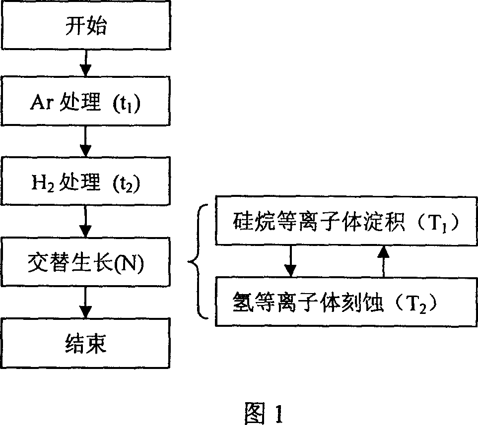
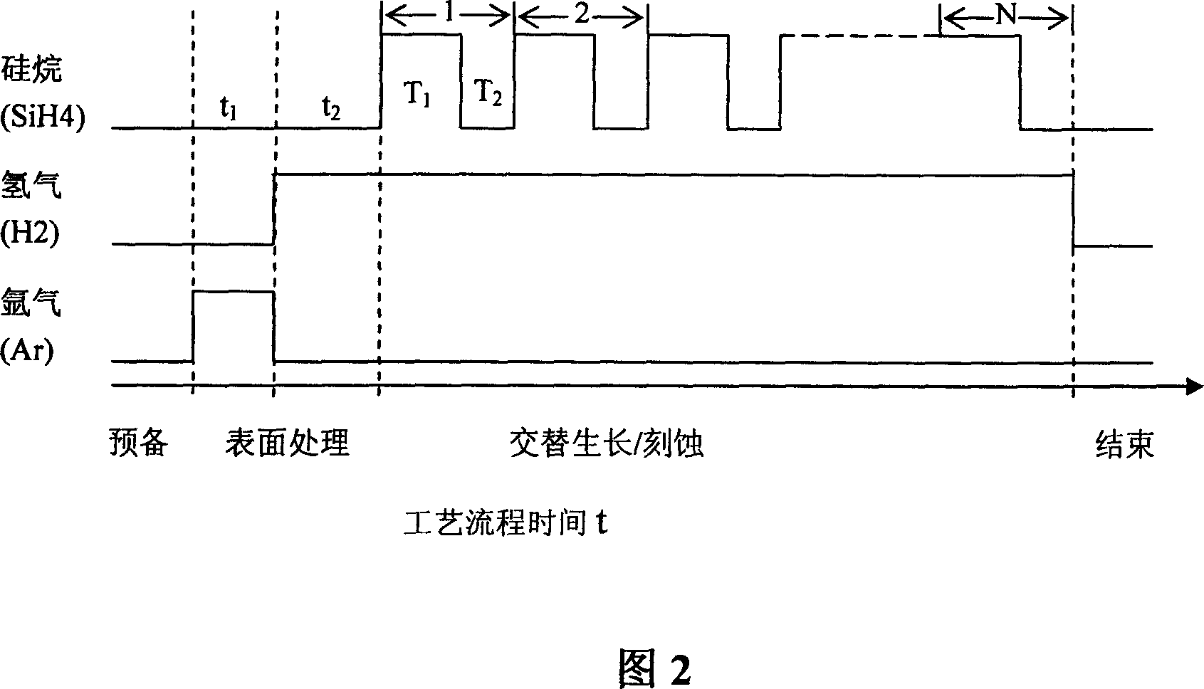
[0026] According to Figures 1 and 2; the first step: pretreatment of the silicon substrate surface:

[0027] Parameters for surface pretreatment with argon and hydrogen plasma:

[0028] First, argon plasma was first used in plasma enhanced chemical vapor deposition (PECVD) systems

[0029] Surface treatment, the specific process conditions are as follows:

[0030] Power source frequency: 13.56MHz, power density: 1W / cm 2

[0031] Reaction chamber pressure: 45Pa, substrate temperature: 200°C

[0032] Processing time: about 300 seconds

[0033] Secondly, hydrogen plasma is used to treat the surface in a plasma-enhanced chemical vapor deposition (PECVD) system, and the specific process conditions are as follows:

[0034] Power source frequency: 13.56MHz, power density: 1.33W / cm 2

[0035] Reaction chamber pressure: 80Pa, substrate temperature: 200°C

[0036] Processing time: 130 seconds

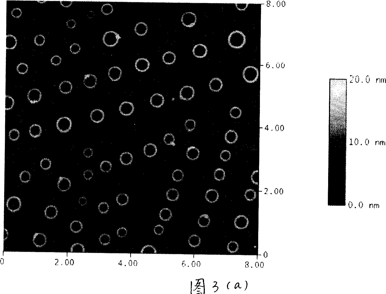
[0037] The second step: use the periodic growth / etching method to grow the Si nanori...


PUM

PropertyMeasurementUnit
heightaaaaaaaaaa
diameteraaaaaaaaaa
diameteraaaaaaaaaa

Abstract

The invention relates to a method for preparing gas self-assemble silicon quantum annular nanometer structure, wherein it comprises that: in the plasma strengthen chemical gas deposit system (PECVD), on the substrate silicon surface, processing the pretreatment of argon plasma and hydrogen plasma, to form the corn center of silicon nanometer ring; the in PECVD system, periodically using hydrogen diluted silane gas (SiH4+H2) and hydrogen gas (H2) to grow and etch the silicon at corn center, to form the silicon quamtum annular nanometer structure; processing surface pretreatment on silicon substrate to form the corn center with nanometer annular structure, while its density is 1-3*108 / cm2. And when grows and etches silicon, in each period, it uses hydrogen diluted silane to grow the corn center, and uses pure hydrogen gas to etch silicon, repeats the deposit and etch periods for 5-50 times.

Description

1. Technical field: [0001] The invention relates to a method for preparing silicon quantum ring nanostructures grown by gas phase self-assembly, and proposes a method for preparing silicon quantum ring nanostructures in a plasma-enhanced chemical vapor deposition (PECVD) system from two aspects of principle and implementation process. A new technique for three-dimensional ordered silicon nanoring structures. 2. Background technology: [0002] The integration of nanoelectronics and optoelectronics based on semiconductor quantum structures is the core of the new generation of semiconductor devices in the 21st century and the hardware foundation of modern information technology. Semiconductor silicon (Si) is currently the most important material for the preparation of microelectronic devices. However, whether Si can continue to play an important role in the era of nanoelectronic devices and whether it can realize Si monolithic optoelectronic integration and electromagnetic regu...

Claims


Application Information

Patent Timeline
Patent Type & Authority Applications(China)
IPC IPC(8): B82B3/00C23C16/513
Inventor 余林蔚陈坤基李伟徐骏黄信凡宋捷李雪飞马忠元徐岭
Owner NANJING UNIV
Why Eureka
Try Eureka