

Semiconductor back-end linked thread using glass contained F-Si as dielectric substance
A dielectric and semiconductor technology, applied in the field of semiconductor back-end connection, can solve the problems of short electromigration life, peeling, electromigration failure, etc., and achieve the effect of high product qualification rate, good integrity, and improved electromigration life
- Summary
- Abstract
- Description
- Claims
- Application Information
AI Technical Summary
Problems solved by technology
Method used
Image

Examples
Embodiment Construction
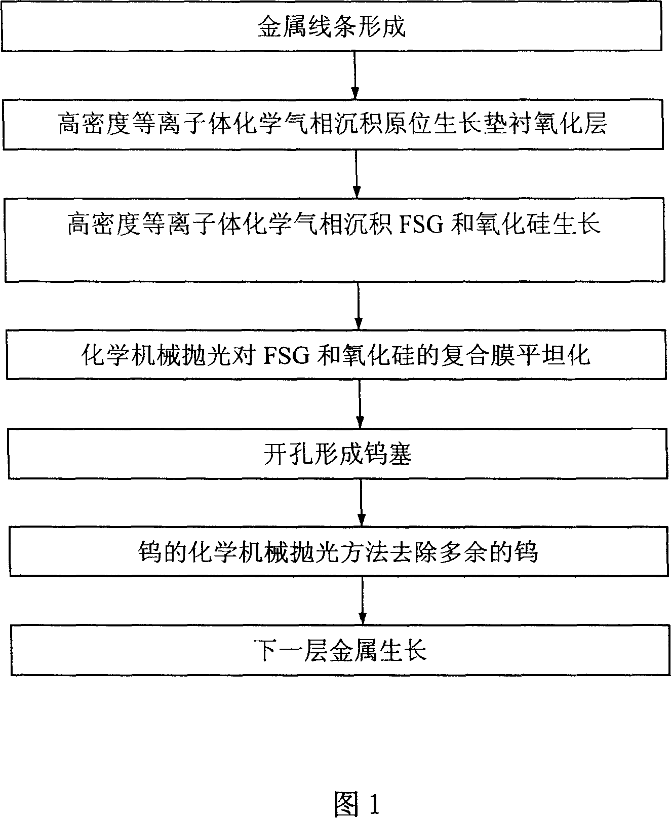
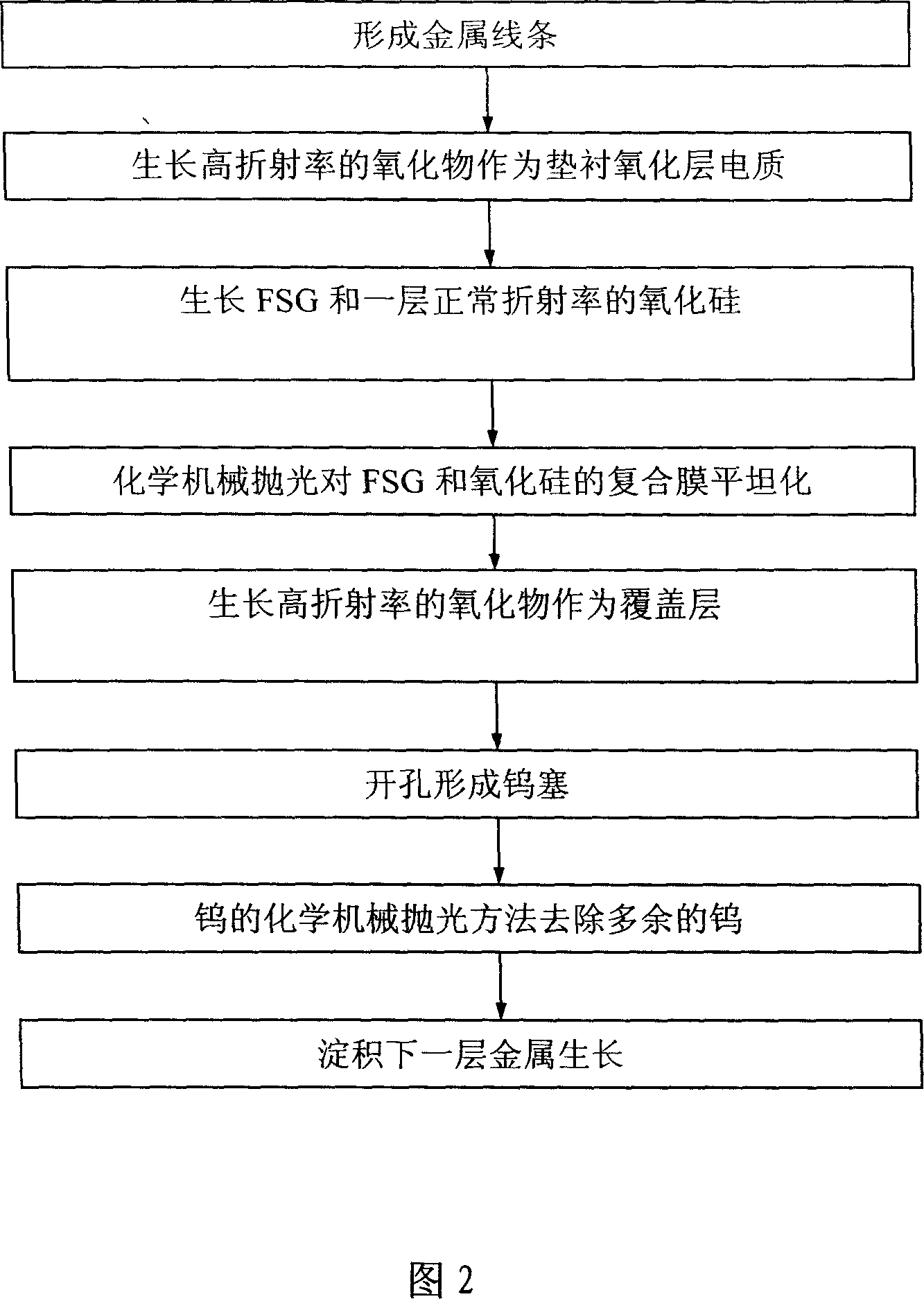
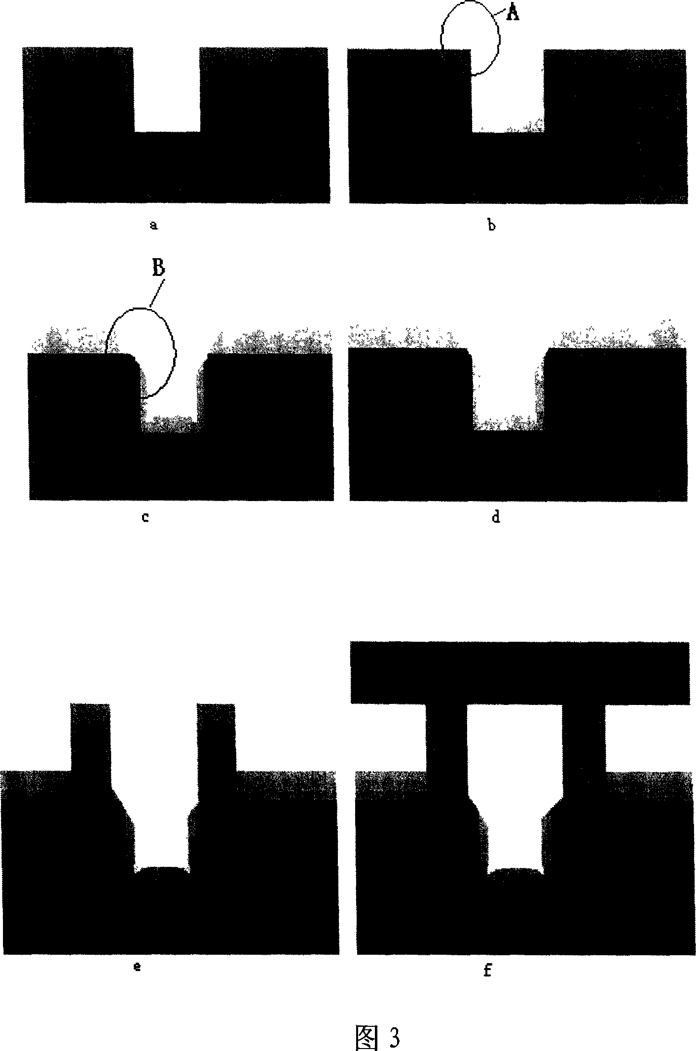
[0019] As shown in Figure 2 and Figure 4, firstly, metal lines are formed, see Figure 4a; secondly, a high-refractive-index oxide grown by plasma-enhanced chemical vapor deposition in PECVD equipment is used as a pad oxide layer, see Figure 4b ; Wherein, the pad oxide layer is silicon oxide, silicon oxynitride, silicon nitride or a combination thereof, the pad oxide film has a refractive index greater than 1.48, and a thickness greater than 12nm and less than 80nm. The third step is to use high-density plasma chemical vapor deposition to grow FSG and deposit FSG as a dielectric, see Figure 4c; the fourth step is to cover the surface with a layer of normal refractive index silicon oxide after the growth of FSG dielectric Or tetraethoxysilane, and then planarize it with chemical mechanical polishing, see Figure 4d. In this step, it is also possible not to cover silicon oxide or tetraethoxysilane, and directly use chemical mechanical polishing to planarize it; the fifth step is t...
PUM
| Property | Measurement | Unit |
|---|---|---|
| Thickness | aaaaa | aaaaa |
| Thickness | aaaaa | aaaaa |
Abstract
Description
Claims
Application Information