Surface nano tip array and its preparing method

A technology of nano cones and arrays, applied in the direction of nanostructure manufacturing, nanotechnology, nanotechnology, etc., can solve the problems of small production area, poor consistency and controllability, poor adhesion, etc., and achieve a wide range of applications and a small radius of curvature at the top Effect

Inactive Publication Date: 2007-06-13
INST OF PHYSICS - CHINESE ACAD OF SCI
View PDF0 Cites 26 Cited by
  • Summary
  • Abstract
  • Description
  • Claims
  • Application Information

AI Technical Summary

Problems solved by technology

[0006] One of the purposes of the present invention: not only overcome the defects of the existing nanocone array prepared by the direct growth method, such as limited range of applicable materials, poor consistency and controllability, low success rate and poor adhesion, but also overcome the existing electrical The aspect ratio of surface nanocone arrays prepared by chemical etching and template methods is too small, the radius of curvature is large, the fabrication area is too small, and the complete electrical information and morphology information cannot be obtained as a probe, as well as in terms of mechanics. The application potential is not large; thereby providing a controllable aspect ratio, controllable density, small tip curvature radius, and a wide range of applicable materials, and can be used for field emission devices, scanning probe systems, Surface nanocone arrays for biosensors, nanoimprinting and optoelectronics

Method used


Image

  • Surface nano tip array and its preparing method
  • Surface nano tip array and its preparing method
  • Surface nano tip array and its preparing method

Examples


Embodiment 1

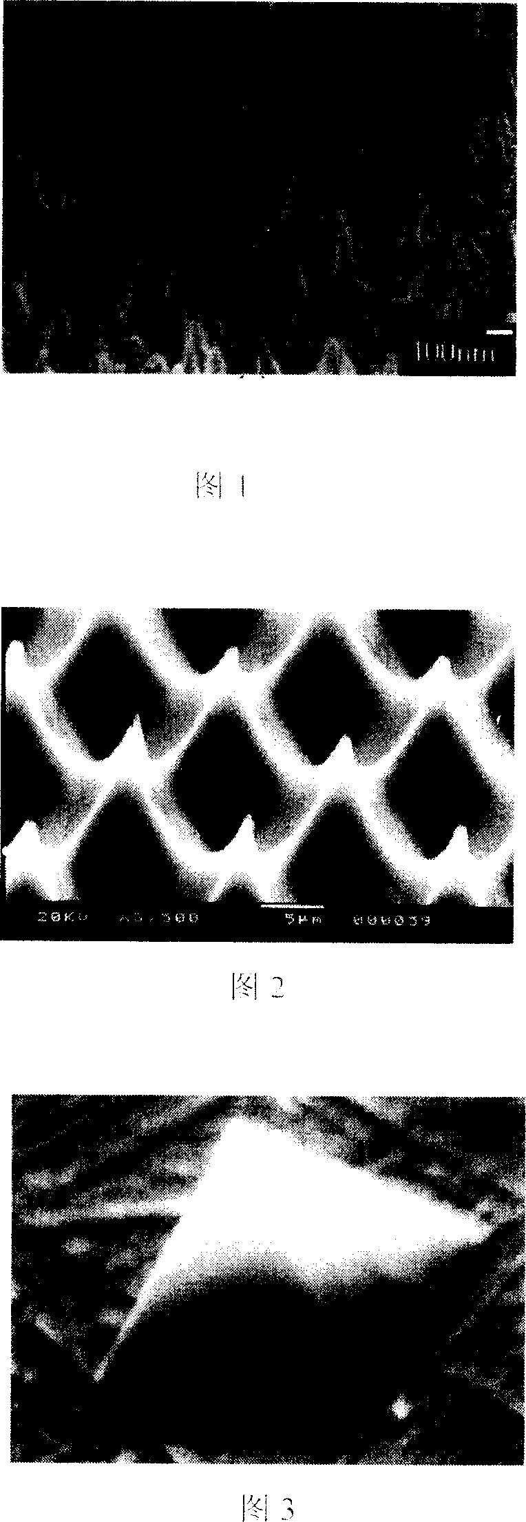
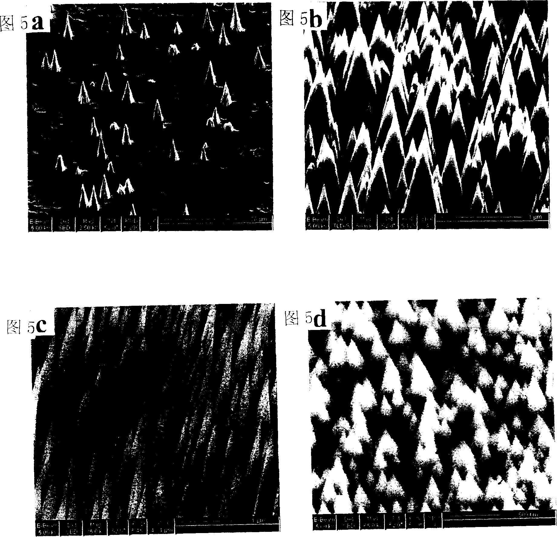
[0043] Referring to Fig. 5a, a diamond surface nanocone array is fabricated. The cone height of the nanocone array on the diamond surface is about 8-10 microns, the tip curvature radius is 5 nanometers, the aspect ratio is about 1600-2000, the bottom diameter is 1-2 microns, the cone angle is about 34°, and the cone density is 2× 10 6 cm -2 .

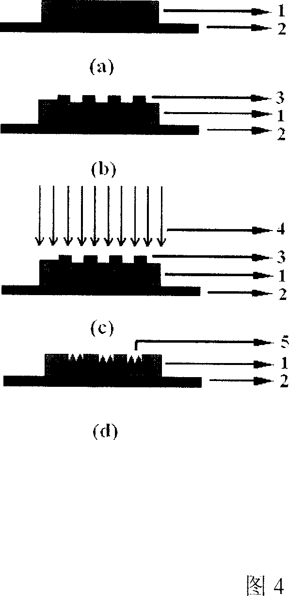
[0044] Referring to Fig. 4a-d, the specific method of the present invention is described in detail according to its process steps.

[0045] 1), using the hot wire CVD method to prepare a diamond thick film with a thickness of about 15 microns on a 3cm×2cm n-type silicon wafer as the etching substrate 1, and ultrasonically treat the silicon wafer for 1 hour by diamond powder grinding before growing, and place The cleaned substrate material 1 is placed on the stainless steel round support 2, and placed in the CVD equipment, and vacuumed to 10 -2 The specific parameters of Torr’s hot wire CVD method growth are as follows: air pressure:...

Embodiment 2

[0053] The specific structure of the diamond surface nanocone array 5 of the present embodiment is referring to Fig. 5 (b); The height of the diamond cone tip is about 1 micron, the radius of curvature of the tip is 2 nanometers, the aspect ratio is about 500, and the bottom diameter is 0.3 micron. Density is 5×10 8 cm -2 .

[0054] Made according to the preparation process of Example 1, the difference between this example and Example 1 is as follows: the volume ratio of methane / hydrogen gas during plasma 4 etching: 1.5 / 98.5, the pressure is 20 Torr, and the time is 1 hour.

Embodiment 3

[0056] The specific structure of the nanocone array 5 on the porous silicon surface of the present embodiment is referring to accompanying drawing 5 (c), and the height of the cone tip is about 2 microns, the radius of curvature of the tip is 5 nanometers, the aspect ratio is about 400, and the diameter of the bottom is 0.3 microns. Density is 4×10 8 cm -2 .

[0057] The difference with embodiment 1 is as follows:

[0058] 1. The present embodiment adopts the porous silicon substrate 1 prepared by the electrochemical etching method, and its specific preparation method is as follows: n-type silicon (6-9Ω.cm): 1cm×1cm, electrochemical etching solution: C 2 h 5 OH / HF (49%) is 1:1 (volume ratio), corrosion time: 15 minutes, corrosion current: 20 mA.

[0059] 2. The volume ratio of methane / hydrogen gas during plasma 4 etching: 2 / 98, the gas pressure is 20 Torr, and the time is 2 hours; due to the good conductivity of porous silicon, this embodiment does not use fine Pt metal wi...


PUM

PropertyMeasurementUnit
diameteraaaaaaaaaa
angleaaaaaaaaaa
diameteraaaaaaaaaa

Abstract

This invention relates to a surface nm cone array and its manufacturing method, in which, said surface nm conical array is formed by applying a plasma etching technology and preparing nm conical array on a substrate with the major diameter ratio between 50-8000, the curvature radius on the tip lower than 5 nm, the bottom diameter of 200-2000 nm, the cone angle of 16-72 deg. and the density of 109 cm2-105 cm2, the preparation method includes: putting it in a CVD device after cleaning the substrate in a biased chemical gas phase deposition device, vacuumizing it to 10-2 Torr, applying plasma pre-etching process, then turning off the bias and filament current then to re-vacuumize it to 10-2 Torr then to etch it to form a surface nm cone array.

Description

technical field [0001] The invention relates to a surface nanocone and a manufacturing method thereof, in particular to a surface fabricated on various solid materials used in fields such as field emission devices, scanning probe systems, biosensors, nanoimprinting and optoelectronics Nanocone array and fabrication method. Background technique [0002] There are roughly three existing techniques for fabricating surface nanocones: direct growth method, electrochemical corrosion method, and template method. Now three kinds of existing techniques for making surface nanocones are specifically described as follows: [0003] 1. Preparation of amorphous carbon nanocones by direct growth method: see Reference 1, "Field emission from amorphous-carbon nanotips on copper", published in Journal of Applied Physics. "2003, Vol.15, No.10: 6796-6799. The amorphous carbon nanocone array is shown in Figure 1. This method uses microwave plasma technology to directly grow amorphous carbon n...

Claims


Application Information

Patent Timeline
Patent Type & Authority Applications(China)
IPC IPC(8): B82B1/00B82B3/00
Inventor 顾长志王强李俊杰王宗利
Owner INST OF PHYSICS - CHINESE ACAD OF SCI
Why Eureka
Try Eureka