

Device structure and its production for single-modulus quantum cascade laser
A technology of quantum cascade and manufacturing method, which is applied to laser components, optical waveguide semiconductor structure, laser, etc., can solve the problems of complex manufacturing process, achieve the effect of simple device process and avoid complex process
- Summary
- Abstract
- Description
- Claims
- Application Information
AI Technical Summary
Problems solved by technology
Method used
Image

Examples
example
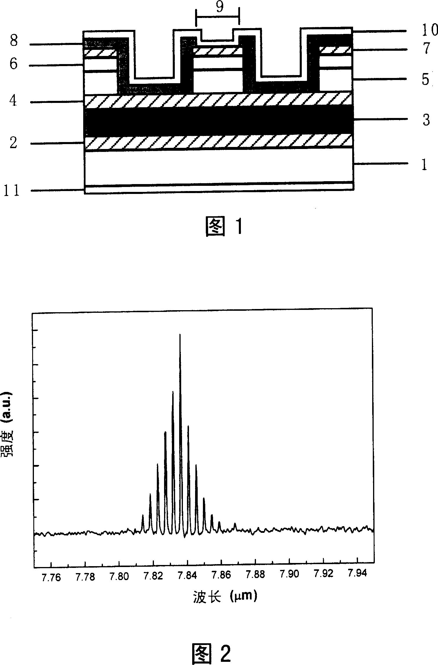
[0063] Please refer to Fig. 1 again, the present invention relates to a kind of device structure of single-mode quantum cascade laser, comprising:
[0064] n-type indium phosphide substrate 1 as the lower cladding layer;
[0065] n-type InGaAs lower waveguide layer 2, the lower waveguide layer 2 is fabricated on the n-type substrate 1, and is used to increase the refractive index of the waveguide core layer and enhance light confinement;
[0066] 35 cycles of alternating InGaAs / InAlAs active layer 3, the active layer 3 is fabricated on the lower waveguide layer 2 as a light-emitting area;
[0067] n-type InGaAs upper waveguide layer 4, the upper waveguide layer 4 is fabricated on the active layer 3, and is used to increase the refractive index of the waveguide core layer and enhance light confinement;
[0068] n-type indium aluminum arsenic upper cladding layer 5, the upper cladding layer 5 is fabricated on the upper waveguide layer 4;
[0069] n-type InGaAs highly doped con...
PUM
 Abstract
Description
Claims
Application Information