Electronic carrier plate and packaging structure thereof

A carrier board and electronic technology, which is applied in the direction of assembling printed circuits, circuits, and electrical components with electrical components. It can solve the problems of small space, short circuit of adjacent passive components, and turbulent flow in the corner of the flow channel, so as to avoid gas explosion and electric shock. The effect of sexual bridging

Inactive Publication Date: 2007-07-04
SILICONWARE PRECISION IND CO LTD
View PDF2 Cites 2 Cited by
  • Summary
  • Abstract
  • Description
  • Claims
  • Application Information

AI Technical Summary

Problems solved by technology

[0012] Please refer to FIG. 4B. In US Patent No. 2005/0253231, when the insulating resin 47 (as shown by the arrow) flows into the two openings 430 formed by the barrier strip 431 and the exposed solder pad 42 When the flow channel is 4300, the space is extremely small, which can easily cause turbulent flow at the corner of the flow channel, and even lead to the generation of air cavity V, which will increase the probability of gas explosion in the subsequent thermal process environment
[0013] Furthermore, in the technologies disclosed in the above-mentioned U.S. Patent No. 6,521,997 and No. 2005/0253231, in the face of the influence of the configuration of adjacent passive components, they

Method used


Image

  • Electronic carrier plate and packaging structure thereof
  • Electronic carrier plate and packaging structure thereof
  • Electronic carrier plate and packaging structure thereof

Examples


Embodiment 1

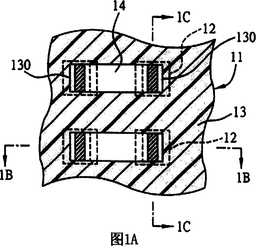
[0036] Please refer to FIG. 5A and FIG. 5B , which are schematic plan views of the electronic carrier board of the present invention and Embodiment 1 of constructing electronic components on the electronic carrier board. It should be noted that the drawings are simplified schematic diagrams, The basic structure of the invention is illustrated by way of illustration only. Therefore, only elements related to the present invention are shown in the drawings, and the number, shape, and size ratio of the shown elements are not drawn in actual implementation, and the layout of the elements may be more complicated.

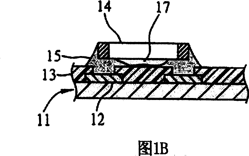
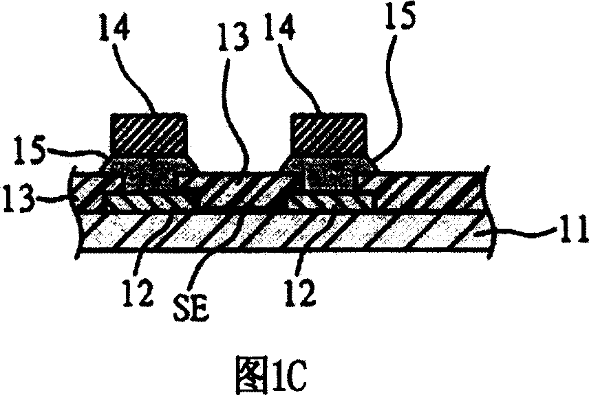
[0037] As shown in the figure, the electronic carrier 51 of the present invention includes: a main body 511; a plurality of welding pads 52 arranged in pairs on the surface of the main body; and a protective layer 53 for covering the surface of the main body 511, the protective layer 53 An opening 54 is formed corresponding to at least two welding pads 52 arranged in pair...

Embodiment 2

[0045] Please refer to FIG. 7 , which is a schematic plan view of Embodiment 2 of the electronic carrier board of the present invention.

[0046] The electronic carrier board and its assembly structure of Embodiment 2 of the present invention are substantially the same as those of Embodiment 1 above, the main difference being that the protective layer 53 on the electronic carrier board is formed in the opening 54 between corresponding paired welding pads 52. A plurality of independent residual portions 530, two independent residual portions 530 are shown in FIG. It can provide good support for the subsequent electronic components, and at the same time provide a flow channel space for the insulating resin without dead ends, so that the insulating resin can flow smoothly and be fully distributed in the openings under the electronic components.

Embodiment 3

[0048] Please refer to FIG. 8 , which is a schematic plan view of Embodiment 3 of the electronic carrier board of the present invention.

[0049] The electronic carrier board and its assembly structure in Embodiment 3 of the present invention are substantially the same as those in Embodiment 1 above, the main difference being that the protective layer 53 on the electronic carrier board is formed in the opening 54 between corresponding pairs of welding pads 52. A plurality of independent residual portions 530, two independent residual portions 530 are shown in FIG. Part of the protective layer 530 is not connected, so as to provide good support for the subsequent electronic components, and provide a flow channel space for the insulating resin without dead ends, so that the insulating resin can flow smoothly and fully distribute in the opening below the electronic components.


PUM


Abstract

The invention relates to an electric carrier, wherein it comprises main body, several welding pads on the face of main body, and a protective layer covering the main body; the protective layer has one cut between two couple welding pad, while at least three side faces are exposed from the welding pads; the protective layer has at least one independent left part between the welding pads; the electric element can connect the left part, to connect the couple welding pads via conductor; the electric element and the face of main body have non-dead-corner channel; insulated resin covers the electric element to be distributed at the low side of electric element and in the open, to cover at least three side faces of welding pad, to avoid generating gas hole at low side of electric element, and avoid bad connection between welding pads or between conductors of nearby electric elements.

Description

technical field [0001] The present invention relates to an electronic carrier board and a structural structure, in particular to an electronic carrier board and a structural structure applied in surface mount technology (Surface Mounted Technology, SMT). Background technique [0002] With the advancement of integrated circuit production technology, the design and production of electronic components continue to develop towards the trend of miniaturization, and because they have larger-scale and highly integrated electronic circuits, the product functions are also more complete. [0003] In this case, the electronic components that are traditionally placed using Through Hole Technology (THT) cannot be further reduced in size, thus occupying a printed circuit board (Printed Circuit Board; PCB), a circuit board (circuit board) ) or substrate (substrate) and other electronic carrier boards have a lot of space, plus the plug-in assembly technology needs to drill holes on the elect...

Claims


Application Information

Patent Timeline
IPC IPC(8): H05K1/00H05K3/30H05K13/00H01L23/02
Inventor 蔡芳霖蔡和易黄致明黄建屏萧承旭
Owner SILICONWARE PRECISION IND CO LTD
Why Eureka
Try Eureka