Te, cadmium and Hg optical range limiter with the continuously adjusting output light intensity of the passive saturated clamp

An output light, passive technology, applied in the structure/shape of lasers, laser parts, optical resonators, etc., can solve the problem that the output light intensity cannot be continuously adjusted.

Inactive Publication Date: 2007-07-11
SHANGHAI INST OF TECHNICAL PHYSICS - CHINESE ACAD OF SCI
0 Cites 6 Cited by

AI-Extracted Technical Summary

Problems solved by technology

Although this method effectively increases the two-photon absorption length of the material, its output ligh...

Abstract

This invention discloses one passive saturation clamp output light intensity continuous adjusting mercury-cadmium-tellurium limit range device, which comprises one pair of Brag reflection lens formed F-P optical resonance chamber and the Hectic photoelectric diode in middle of F-P optical resonance chamber middle as absorptive layer and the direct current stable power exerted onto diode.

Application Domain

Optical resonator shape and constructionNon-linear optics +1

Technology Topic

Wave bandHigh power lasers +13

Image

  • Te, cadmium and Hg optical range limiter with the continuously adjusting output light intensity of the passive saturated clamp

Examples

  • Experimental program(1)

Example Embodiment

[0015] In the following, the incident wavelength 7920nm is taken as the design wavelength, and the details of the optical limiter of the present invention are described in conjunction with the drawings.
[0016] Detailed description of the implementation mode:
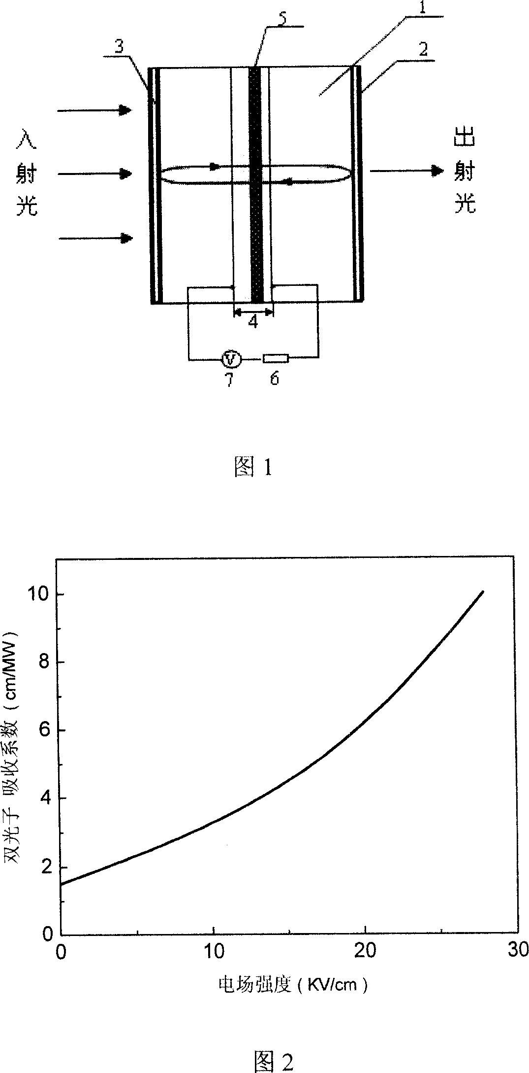
[0017] The resonant cavity 1 of the HgCdTe optical limiter of the present invention is composed of a pair of distributed Bragg reflectors 2, two opposing mirror surfaces are plated with (HL)m or (LH)m dielectric films 3, and the mirror substrate material is Ge, H Is the high refractive index film layer SiO, L is the low refractive index film layer PbTe, the refractive index of which is 2.35 and 5.55, respectively, m is the number of alternating layers of high and low refractive index film layers, m=2, the optical thickness of the film layer is λ 0 /4, the length of the resonant cavity is 7.92mm. The HgCdTe photodiode 4 is placed in the resonant cavity, and the space charge region 5 in the p-n junction of the photodiode is the center of the resonant cavity to achieve the best optical limiting effect. For the incident wavelength of 7920nm, the transmitted light width of this resonant cavity structure is 2.3nm and the center wavelength is 7920nm, as shown in Figure 1.
[0018] HgCdTe photodiode 4 as a light absorbing material is a key part of the limiter. It is a narrow band gap semiconductor material. The light absorption mainly occurs in the infrared band. The light in the near, middle and far infrared bands can be obtained by adjusting the Cd component. Limiting absorption. Corresponding to this example, if the incident fundamental frequency photon energy is 60% of the HgCdTe band gap, the corresponding Cd composition is 0.305. The preparation method is to use molecular beam epitaxy to grow on the CdTe buffer layer with GaAs substrate to form a p-type epitaxial layer, and implant boron ions on the surface to form n + Type mutation n + -p junction, and then deposit a CdTe passivation layer on its surface to minimize surface recombination. In order to meet the limitation of high-power pulsed laser beam, n + The effective area of ​​the -p junction should be larger than the laser spot diameter, here is 2×2cm.
[0019] The electrode lead wire of the HgCdTe photodiode is connected to the DC stabilized power supply 7 through the load resistance 6. The load resistance protects the HgCdTe photodiode, and the stabilized DC power supply is added to the n + -The p junction forms a reverse bias mode. Because n + When the p junction is in reverse bias, the input impedance relative to the load resistance is very large. It can be considered that the output voltage of the DC power supply is all added to the space charge area. + -The electric field strength on the p junction. When the electric field strength tilts the energy band of the material to a certain extent, the Franz-Keldysh effect modulates the effective band gap of the material, and the incident photon changes relative to the effective band gap of the material. In order to adjust the second-order absorption coefficient of the material artificially, the output light intensity of the optical limiter changes accordingly. The F-P resonant cavity enhances the absorption efficiency of the absorbing material for incident light.
[0020] In the design process, due to optical absorption loss material n + -The breakdown voltage that the p junction can withstand is limited, and excessive external bias will cause n + -The breakdown of the p junction, the large reverse current makes the field strength of the space charge zone no longer increase, so the excessive reverse bias can no longer artificially adjust the output light intensity. Therefore, in this example, according to the breakdown electric field strength, the maximum external bias voltage should not exceed -1V. + The electric field intensity at the -p junction has been greater than 30kV/cm, and the two-photon absorption coefficient has been increased by 7 times relative to the zero bias condition. Therefore, with the present invention, the limiting capability of the optical limiter can be tuned about 5 times.

PUM

no PUM

Description & Claims & Application Information

We can also present the details of the Description, Claims and Application information to help users get a comprehensive understanding of the technical details of the patent, such as background art, summary of invention, brief description of drawings, description of embodiments, and other original content. On the other hand, users can also determine the specific scope of protection of the technology through the list of claims; as well as understand the changes in the life cycle of the technology with the presentation of the patent timeline. Login to view more.
Why Eureka
Try Eureka