

Electronic carrier board and its packaging structure
A carrier board and electronic technology, which is applied in the direction of assembling printed circuits, circuits, and electrical components with electrical components, which can solve the problem that the encapsulation resin at the bottom of passive components cannot flow in, avoid gas explosion and electrical bridging problems, and prevent improper electrical The effect of sexual bridging
- Summary
- Abstract
- Description
- Claims
- Application Information
AI Technical Summary
Problems solved by technology
Method used
Image

Examples
Embodiment 1
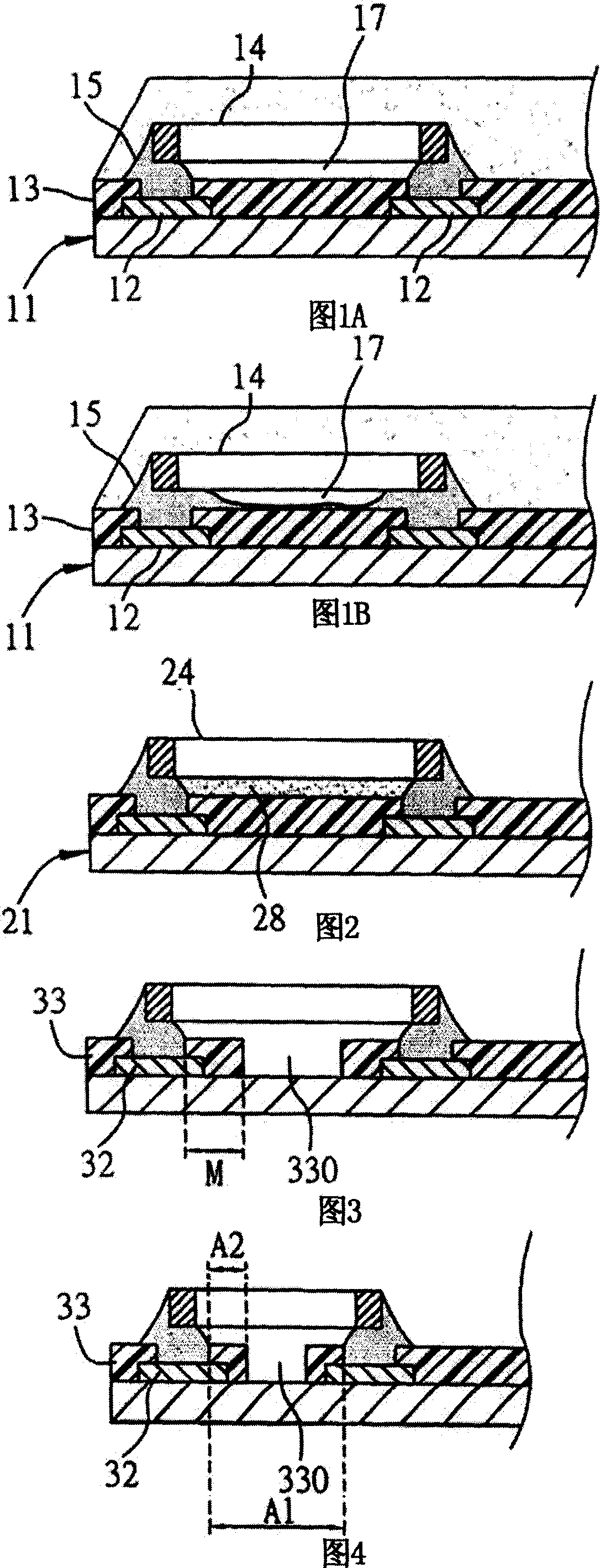
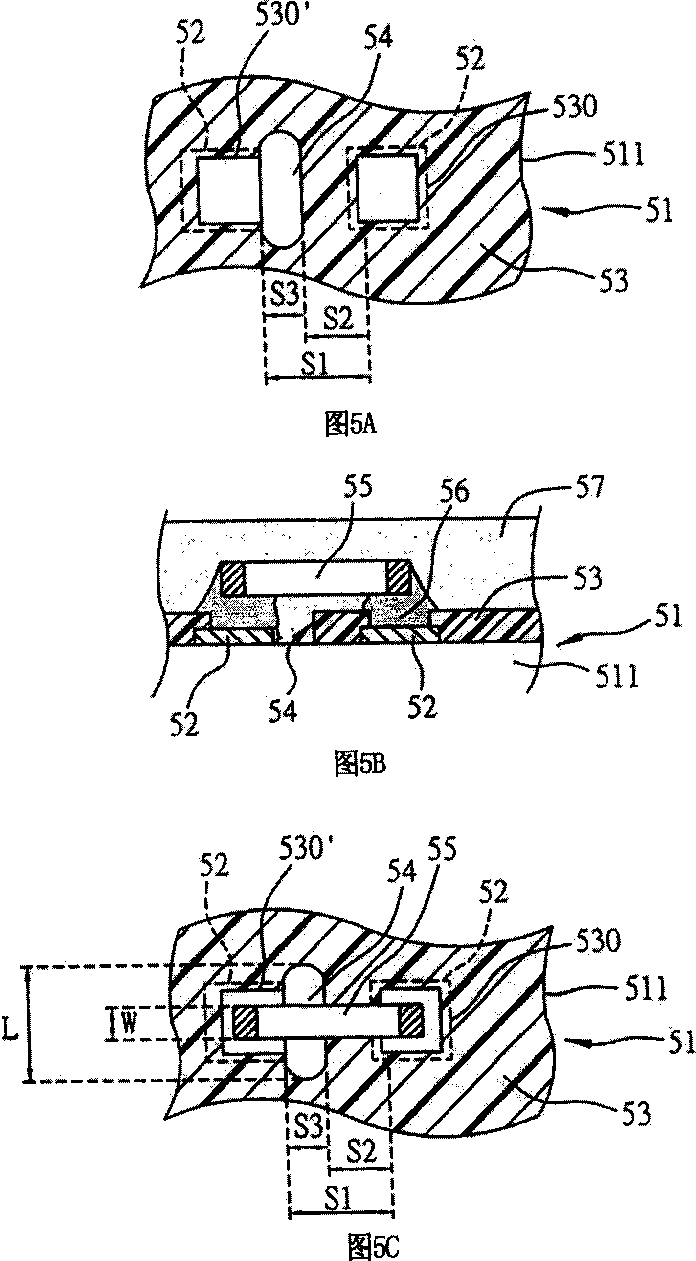
[0044] Please refer to FIG. 5A, FIG. 5B, and FIG. 5C, which are a schematic plan view of Embodiment 1 of the electronic carrier board of the present invention, and a schematic cross-sectional and plan view of Embodiment 1 of electronic components assembled on the electronic carrier board. Among them, it should be noted that Yes, the drawings are all simplified schematic diagrams, only illustrating the basic structure of the present invention in a schematic manner. Therefore, only elements related to the present invention are shown in the drawings, and the number, shape, and size ratio of the shown elements are not drawn in actual implementation, and the layout of the elements may be more complicated.
[0045] As shown in the figure, the electronic carrier 51 of the present invention includes: a body 511; a plurality of welding pads 52 arranged in pairs on the surface of the body 511; and a protective layer 53 for covering the surface of the body, the protective layer 53 Openin...
Embodiment 2
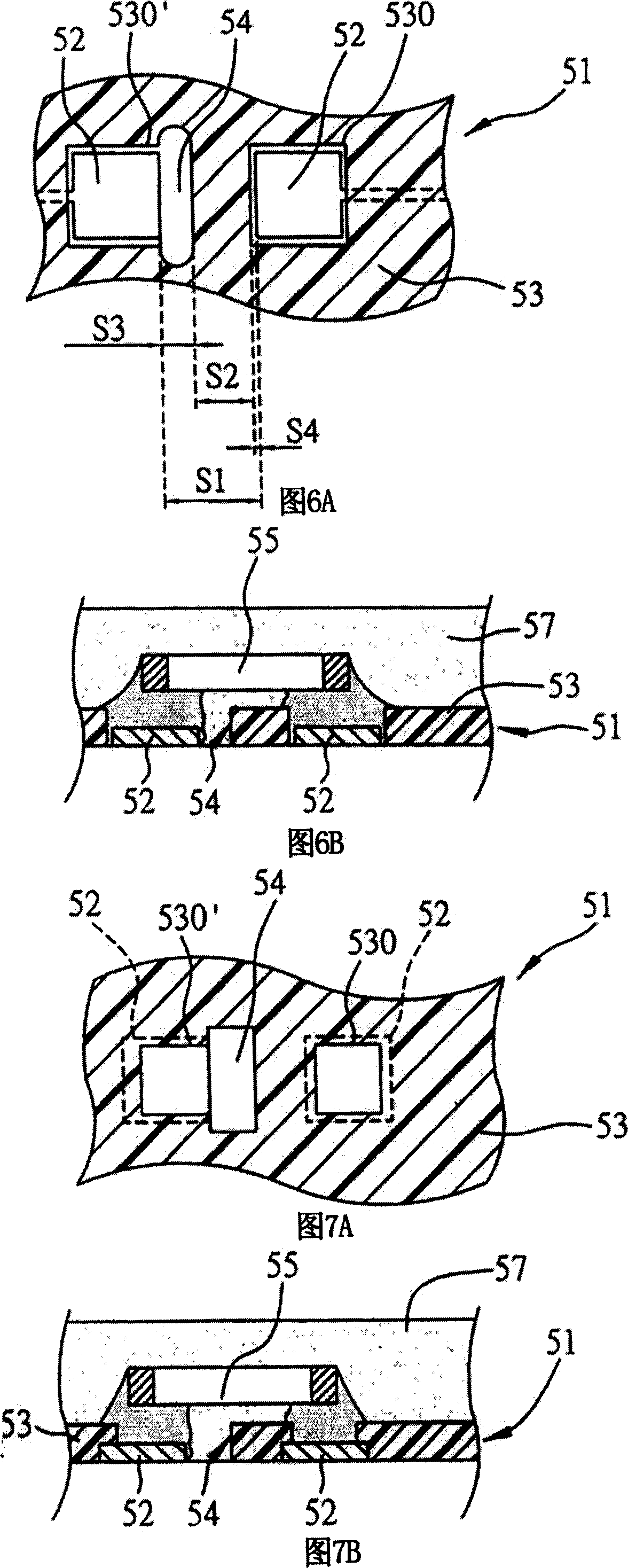
[0055] Please refer to FIG. 6A and FIG. 6B , which are schematic plan views of Embodiment 2 of the electronic carrier board of the present invention, and a schematic cross-sectional view of Embodiment 2 of constructing electronic components on the electronic carrier board.
[0056] The electronic carrier board and its assembly structure of Embodiment 2 of the present invention are substantially the same as those of Embodiment 1 above, the main difference is that the corresponding openings 530, 530' formed in the protective layer (solder resist layer) 53 are larger in size than the solder pads 52 is of such a size that the solder pad 52 completely exposes the protection layer 53, thereby forming a non-solder mask defined (NSMD) solder pad.
[0057] Similarly, when a passive component such as a 0201 type chip is correspondingly connected, the distance S1 between the exposed pads 52 is 250 microns, and the distance S4 between the edge of the opening 530 and the edge of the non-sol...
Embodiment 3
[0059] Please refer to FIG. 7A and FIG. 7B , which are schematic plan views of Embodiment 3 of the electronic carrier board of the present invention, and schematic cross-sectional views of Embodiment 3 of constructing electronic components on the electronic carrier board.
[0060] The electronic carrier board and its assembly structure of Embodiment 3 of the present invention are substantially the same as Embodiment 1 above, the main difference is that the groove 54 is rectangular.
[0061] It should also be noted that the solder pads 52 exposed from the protection layer 53 may be solder mask defined solder pads or non-solder mask defined solder pads, which are not limited by this drawing.
PUM
 Abstract
Description
Claims
Application Information