
High-power and high-frequency heterostructure field-effect transistor

a heterostructure field-effect transistor and high-power technology, applied in the direction of semiconductor/solid-state device manufacturing, electrical apparatus, semiconductor devices, etc., can solve the problems of complex manufacturing process, low efficiency, and low efficiency of sloped field plates

Active Publication Date: 2018-08-14
STMICROELECTRONICS SRL
View PDF5 Cites 5 Cited by
  • Summary
  • Abstract
  • Description
  • Claims
  • Application Information

AI Technical Summary

Benefits of technology

The patent describes a method for making a field plate in semiconductor devices. The method involves etching the dielectric layer overlying the gate, drain, and source regions to create a cavity with stepping surfaces. These surfaces have different distances from the underlying wafer, resulting in a discontinuous surface. The technical effect of this method is creating a field plate that has improved performance and stability.

Problems solved by technology

High-electron-mobility transistors (HEMTs) based on AlGaN / GaN are generally grown on a silicon substrate, since cheap substrates based of gallium nitride (GaN) are not available.
Without an appropriate shaping of the existing electrical field, in fact, the latter may cause injection of electrons in traps, thus degrading the output current and the on-state resistance during switching.
However, also the solution with sloped field plate is not free from disadvantages.
In fact, it involves a complex manufacturing process and a final planarization step.
Forming the sloped field plate is thus costly and may not be sufficiently controllable.

Method used


Image

  • High-power and high-frequency heterostructure field-effect transistor
  • High-power and high-frequency heterostructure field-effect transistor
  • High-power and high-frequency heterostructure field-effect transistor

Examples


Embodiment Construction

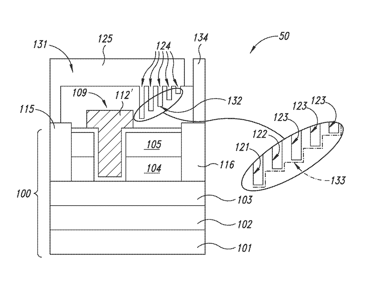
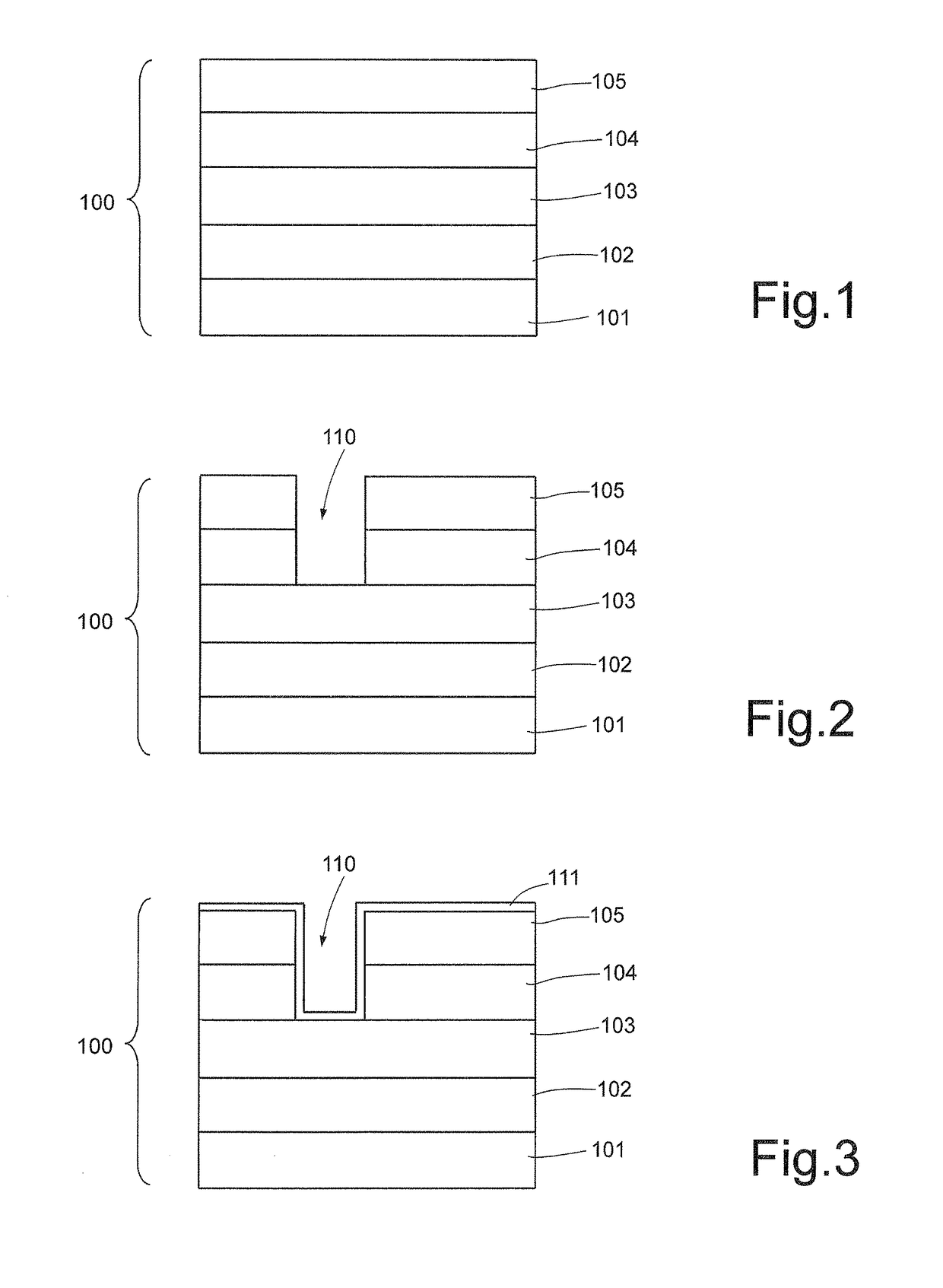
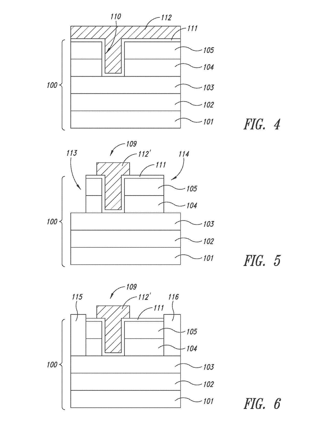
[0018]FIG. 1 shows a portion of a wafer 100 for manufacturing an HEMT device, according to one embodiment of the present device. In particular, the described embodiment regards a heterostructure field-effect transistor of AlGaN / GaN.

[0019]The wafer 100 comprises a substrate 101 of, e.g., silicon, silicon carbide (SiC), or sapphire (Al2O3), overlaid by a buffer layer 102, for example of aluminum gallium nitride (AlGaN) or of indium gallium nitride (InGaN). A channel layer 103 extends on the buffer layer 102 and is here of intrinsic gallium nitride (GaN), having a thickness of, e.g., ca. 10 nm to ca. 10 μm. A barrier layer 104, here of aluminum and gallium nitride (AlGaN) of an intrinsic type, extends on the channel layer 103, in contact therewith, and has a thickness of, e.g., ca. 5 nm and ca. 400 nm. A passivation layer 105 of dielectric material such as silicon nitride (Si3N4) or silicon oxide (SiO2) extends on the barrier layer 104.

[0020]As shown in FIG. 2, the passivation layer 10...


PUM


Abstract

In an HEMT device, a gate region is formed in a wafer having a channel layer, a barrier layer, and a passivation layer, overlying each other. Drain and source electrodes are formed in the wafer, on different sides of the gate region. A dielectric layer is formed over the gate region and over the passivation layer. Selective portions of the dielectric layer are removed by a plurality of etches so as to form one or more cavities between the gate region and the drain electrode. The one or more cavities have a plurality of steps at an increasing distance from the wafer moving from the gate region to the drain electrode. The cavity is then filled with conductive material to form a field plate coupled to the source electrode, extending over the gate region, and having a surface facing the wafer and having a plurality of steps.

Description

BACKGROUNDTechnical Field[0001]The present disclosure relates to a high-power and high-frequency heterostructure field-effect transistor.Description of the Related Art[0002]As is known, AlGaN / GaN heterostructures have drawn high interest for manufacturing high-power and high-frequency field-effect transistors, by virtue of the high breakdown voltage of the material and the high density and mobility of carrier ions in the two-dimensional electron gas (2DEG).[0003]High-electron-mobility transistors (HEMTs) based on AlGaN / GaN are generally grown on a silicon substrate, since cheap substrates based of gallium nitride (GaN) are not available. Therefore, the device is horizontal and the source, drain, and gate electrodes are arranged on the upper surface of the wafer. Thus, the wafer breakdown voltage is linked both to the vertical breakdown voltage and to the lateral distance between the source and the drain electrodes.[0004]Although gallium nitride and its alloys are wide band-gap and h...

Claims


Application Information

Patent Timeline
Patent Type & Authority Patents(United States)
IPC IPC(8): H01L31/0256H01L29/40H01L29/66H01L29/20H01L29/778H01L29/417H01L29/423
CPCH01L29/778H01L29/2003H01L29/402H01L29/66462H01L29/7786H01L29/66431H01L29/4236H01L29/41766H01L21/28
Inventor IUCOLANO, FERDINANDO
Owner STMICROELECTRONICS SRL
Learn More