
Method for manufacturing epitaxial silicon wafer

a manufacturing method and technology of epitaxial silicon, applied in the direction of polycrystalline material growth, crystal growth process, after-treatment details, etc., can solve the problem of complicated temperature regulation, and achieve the effect of preventing the haze of epitaxial silicon wafer and restraining the occurrence of slip dislocation

Active Publication Date: 2019-04-09
SUMCO CORP
View PDF21 Cites 0 Cited by
  • Summary
  • Abstract
  • Description
  • Claims
  • Application Information

AI Technical Summary

Benefits of technology

This method effectively reduces the number of SF on epitaxial silicon wafers, achieving low substrate resistivity while simplifying the process and ensuring high-quality wafer production, even with extremely low resistivity silicon wafers, by using hydrogen chloride gas for pre-baking treatments and optimizing the thickness of the outer layer for etching.

Problems solved by technology

The manufacturing method as disclosed in Patent Literature 1 may, however, require a complicated temperature regulation during the pull-up step of the single crystal ingot.

Method used


Image

  • Method for manufacturing epitaxial silicon wafer
  • Method for manufacturing epitaxial silicon wafer
  • Method for manufacturing epitaxial silicon wafer

Examples


Embodiment Construction

)

[0075]Exemplary embodiment(s) of the invention will be described below with reference to the attached drawings.

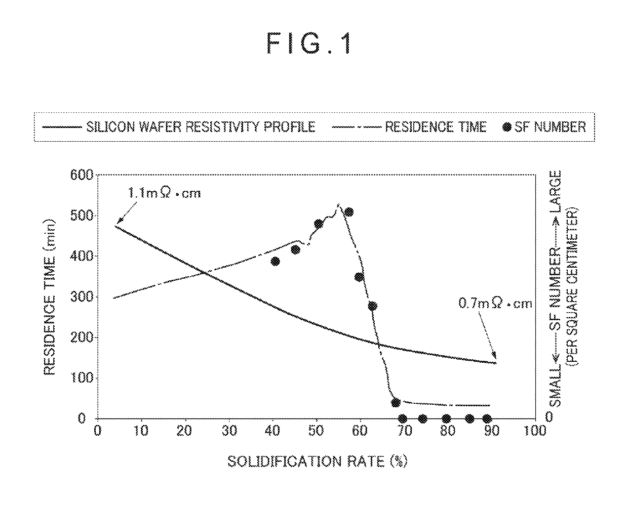
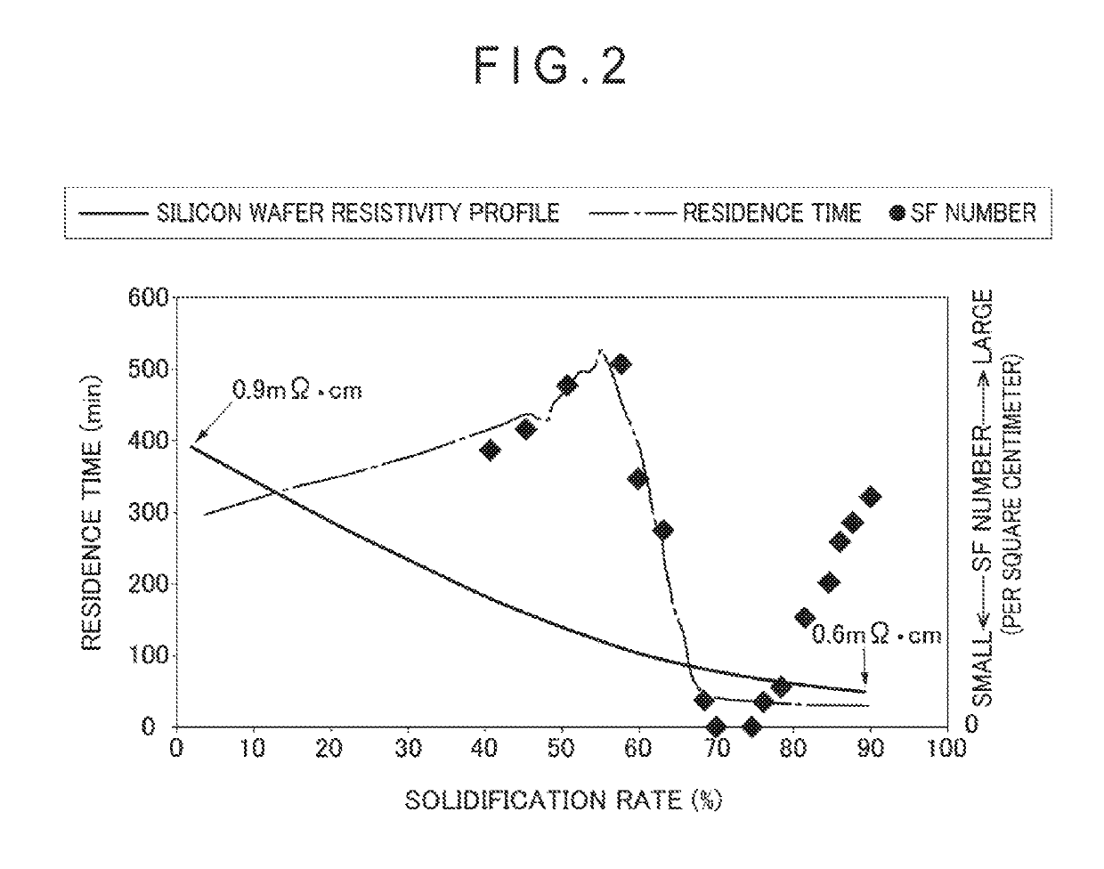
[0076]As shown in FIG. 6, a single crystal ingot manufacturing step (step S1) is conducted in the manufacturing method of an epitaxial silicon wafer.

[0077]In the single crystal ingot manufacturing step, a single crystal ingot with a diameter of 200 mm is manufactured from a silicon melt added with red phosphorus (n-type dopant) according to CZ method (Czochralski process) using a pull-up device (not shown).

[0078]In this exemplary embodiment, the single crystal ingot is manufactured according to the following conditions so that the resistivity of silicon wafers cut out from the single crystal ingot falls in a range from 0.6 mΩ·cm to 0.98 mΩ·cm.

[0079]Red phosphorus concentration: 7.54×10¹⁹ atoms / cm3 or more and 1.32×10²⁰ atoms / cm3 or less

[0080]Oxygen concentration: 7×10¹⁷ atoms / cm3 or more and 12×1017 atoms / cm3 or less

[0081]In order to restrain a misfit dislocation, germaniu...


PUM

PropertyMeasurementUnit
thicknessaaaaaaaaaa
resistivityaaaaaaaaaa
sizeaaaaaaaaaa

Abstract

A method includes: a step of forming an oxide film on a backside of a silicon wafer; a step of removing the oxide film present at an outer periphery of the silicon wafer; a step of argon annealing in which a heat treatment is performed in an argon gas atmosphere; and a step of forming an epitaxial film on a surface of the silicon wafer, the step of forming the epitaxial film including: a step of pre-baking in which the silicon wafer is subjected to a heat treatment in an gas atmosphere containing hydrogen and hydrogen chloride to etch an outer layer of the silicon wafer; and a step of growing the epitaxial film on the surface of the silicon wafer.

Description

TECHNICAL FIELD[0001]The present invention relates to a manufacturing method of an epitaxial silicon wafer.BACKGROUND ART[0002]Epitaxial silicon wafers for power MOS transistors, for instance, are required to have extremely low substrate resistivity. In order to sufficiently lower the substrate resistivity of silicon wafers, it is known to dope molten silicon with an n-type dopant for resistivity adjustment (e.g. arsenic (As) and antimony (Sb)) during a pull-up step (i.e. in growing silicon crystal) of a single crystal ingot for providing silicon wafers (referred to as a single crystal ingot hereinafter). However, since such dopants are extremely volatile, it is difficult to sufficiently increase the dopant concentration in the silicon crystals. Thus, silicon wafers exhibiting desired sufficiently low resistivity is difficult to be manufactured.[0003]Accordingly, silicon wafers with extremely low substrate resistivity have come to be used in which phosphorus (P) as an n-type dopant,...

Claims


Application Information

Patent Timeline
Patent Type & Authority Patents(United States)
IPC IPC(8): H01L21/324C30B25/18C30B29/06C30B33/02C30B33/12H01L21/02C30B25/20
CPCC30B25/186C30B25/20C30B29/06C30B33/02C30B33/12H01L21/324H01L21/0262H01L21/02381H01L21/02532H01L21/02576H01L21/02658H01L21/02019H01L21/02002
Inventor NONAKA, NAOYAKAWASHIMA, TADASHI
Owner SUMCO CORP
Learn More