High efficiency visible and ultraviolet nanowire emitters

a visible and ultraviolet nanowire and emitter technology, applied in the direction of semiconductor laser arrangement, semiconductor laser structure details, semiconductor lasers, etc., can solve the problems of difficult realization of electrically injected semiconductor lasers or efficient light emitting diodes, low output power, and realization of electrically injected quantum dot lasers in the deep uv band. achieve the effect of suppressing non-radiative surface recombination

Active Publication Date: 2019-05-14
MCGILL UNIV
View PDF0 Cites 3 Cited by
  • Summary
  • Abstract
  • Description
  • Claims
  • Application Information

AI Technical Summary

Benefits of technology

[0013]In accordance with an embodiment of the invention there is provided a method of forming atomic scale compositional modulations within a compound semiconductor nanowire to form three dimensional quantum confinement of charge carriers by increasing the concentration of a predetermined element within the composition of the compound semiconductor above a threshold.
[0022]In accordance with an embodiment of the invention there is provided a method of suppressing non-radiative surface recombination within a structure formed from a compound semiconductor comprising at least a predetermined first Group III element, a predetermined second Group III element, and a predetermined Group V element by establishing within a predetermined portion of the structure a region richer in concentration of the predetermined first Group III element within a core region of the structure than an outer region of the structure and richer in concentration of the predetermined second Group III element within the outer region of the structure than the core region of the structure.

Problems solved by technology

Despite the progress in electrically injected semiconductor lasers in the visible, infrared, and terahertz wavelength ranges it has remained difficult to realize electrically injected semiconductor lasers or efficient light emitting diodes (LEDs) within the rich deep ultraviolet (UV) spectrum 10-21.
However, the relatively small lattice mismatch (a maximum of 3% between GaN and AlN), has to date prohibited the realization of electrically injected quantum dot lasers in the deep UV band.
Recent studies have shown that the surface charge properties play a dominant role on the device performance such that for the commonly reported axial nanowire LED designs they exhibit very low output power as a result of the large surface recombination and resulting poor carrier injection efficiency.
However, such radial variations were found to be insufficient to suppress non-radiative surface recombination under electrical injection.
However, each approach leads to increased complexity in the device design, growth and fabrication processes thereby reducing yield / performance and increasing costs for devices.
Moreover, a fundamental understanding of the impact of the AlGaN shell structure on the carrier dynamics and device performance has remained elusive.

Method used


Image

  • High efficiency visible and ultraviolet nanowire emitters
  • High efficiency visible and ultraviolet nanowire emitters
  • High efficiency visible and ultraviolet nanowire emitters

Examples


Embodiment Construction

[0066]The present invention is directed to semiconductor nanowire devices and more particularly to ultraviolet emitters, self-organized nanoclusters, Anderson localization, and self-organized elementally rich shells.

[0067]The ensuing description provides exemplary embodiment(s) only, and is not intended to limit the scope, applicability or configuration of the disclosure. Rather, the ensuing description of the exemplary embodiment(s) will provide those skilled in the art with an enabling description for implementing an exemplary embodiment. It being understood that various changes may be made in the function and arrangement of elements without departing from the spirit and scope as set forth in the appended claims.

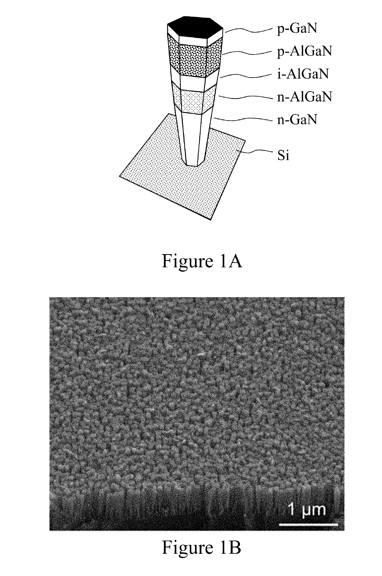
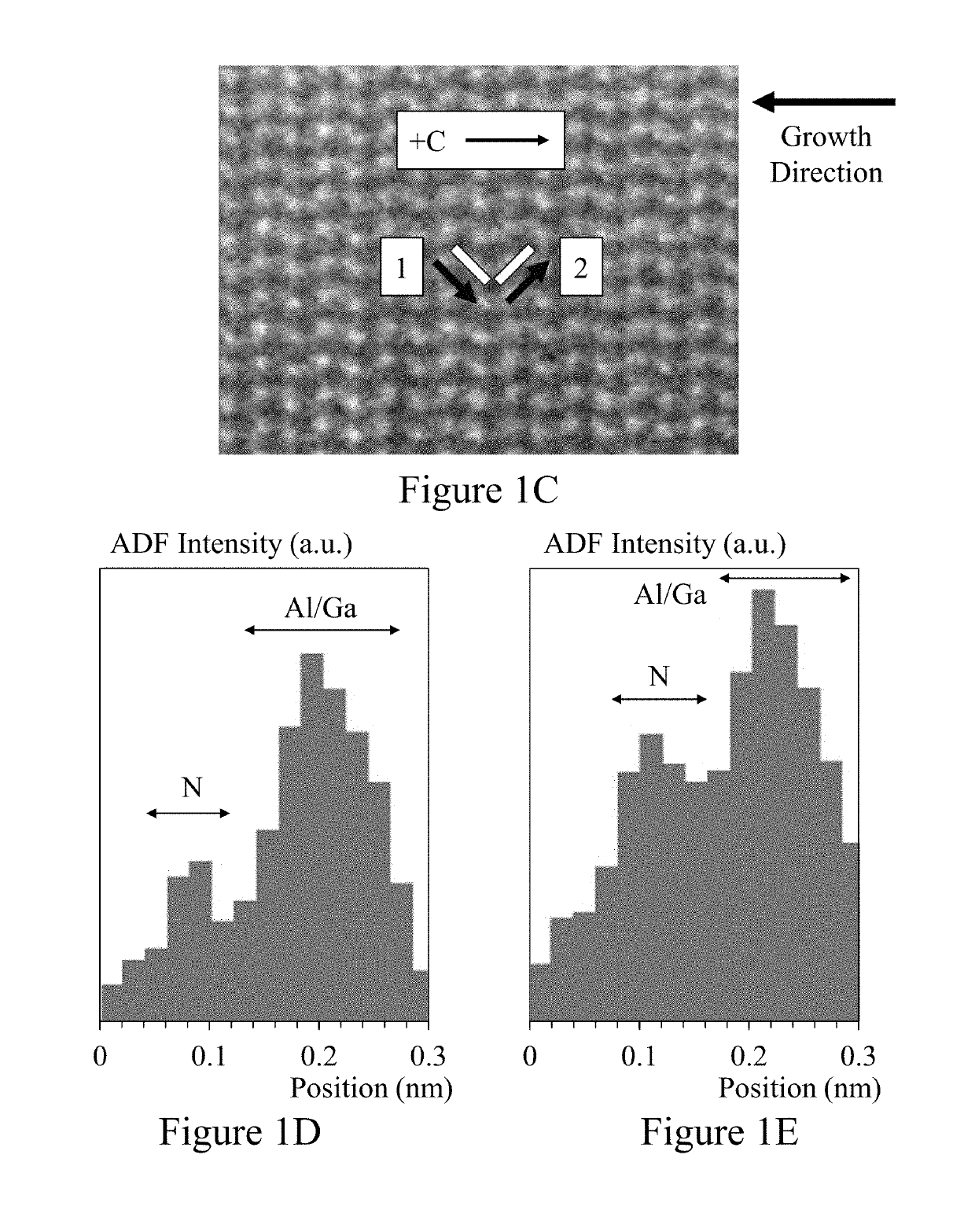
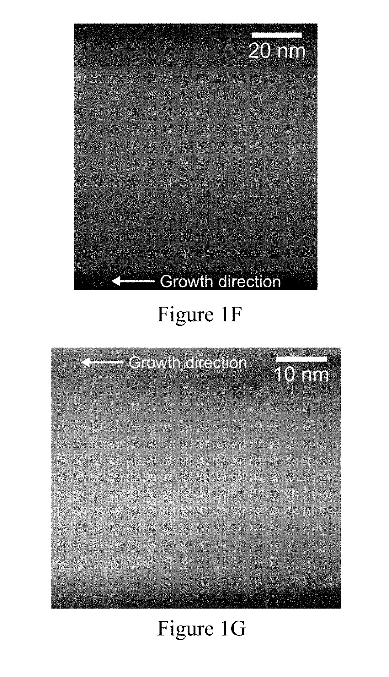
A. Ultraviolet Nanowire Light Source

[0068]A1. Fabrication

[0069]The inventors grew catalyst-free AlGaN nanowires directly onto Si substrates using a radio frequency plasma-assisted molecular beam epitaxy (MBE) system under nitrogen rich conditions. The Si wafers were cleane...


PUM


Abstract

GaN-based nanowire heterostructures have been intensively studied for applications in light emitting diodes (LEDs), lasers, solar cells and solar fuel devices. Surface charge properties play a dominant role on the device performance and have been addressed within the prior art by use of a relatively thick large bandgap AlGaN shell covering the surfaces of axial InGaN nanowire LED heterostructures has been explored and shown substantial promise in reducing surface recombination leading to improved carrier injection efficiency and output power. However, these lead to increased complexity in device design, growth and fabrication processes thereby reducing yield / performance and increasing costs for devices. Accordingly, there are taught self-organizing InGaN / AlGaN core-shell quaternary nanowire heterostructures wherein the In-rich core and Al-rich shell spontaneously form during the growth process.

Description

CROSS-REFERENCE TO RELATED APPLICATIONS[0001]This application claims the benefit of priority from U.S. Provisional Patent Application Ser. No. 62 / 172,874 filed Jun. 9, 2015 entitled “High Efficiency Visible and Ultraviolet Nanowire Emitters.”STATEMENT OF GOVERNMENT INTEREST[0002]This invention was made with U.S. Government support under grant W911NF-12-1-0477 awarded by U.S. Army Research Office. The U.S. Government has certain rights in this invention.FIELD OF THE INVENTION[0003]This invention relates to semiconductor nanowire devices and more particularly to ultraviolet emitters, self-organized nanoclusters, Anderson localization, and self-organized elementally rich shells.BACKGROUND OF THE INVENTION[0004]Compound semiconductor nanowire structures allow broad spectrum photonic devices to be implemented with a single growth process thereby greatly increasing the efficiency of devices exploiting them such as solar cells and light emitting diodes (LEDs), for example, and reducing the...

Claims


Application Information

Patent Timeline
Patent Type & Authority Patents(United States)
IPC IPC(8): H01L33/06H01L33/32H01L33/08H01L33/00H01S5/323H01S5/10H01L33/18H01S5/40H01S5/02
CPCH01L33/06H01L33/007H01L33/08H01L33/18H01S5/1042H01S5/32341H01L33/32H01S5/4006H01S5/021
Inventor MI, ZETIANZHAO, SONGRUIWANG, RENJIE
Owner MCGILL UNIV
Why Eureka
Try Eureka