Group III nitride semiconductor luminescence element
a luminescence element and nitride technology, applied in the field of group iii nitride semiconductor luminescence element, can solve the problem that the yield of ultraviolet ray emitting element having the luminescence peak wavelength of 200 to 350 nm tends to decrease, and achieves the effect of increasing the driving voltage of the element, reducing the quality damage caused by the current concentration near the mesa edge when running the current, and improving the yield of the luminescence elemen
- Summary
- Abstract
- Description
- Claims
- Application Information
AI Technical Summary
Benefits of technology
Problems solved by technology
Method used
Image
Examples
example
[0141]Next, the present invention will be described in further detail by the examples; however the present invention is not to be limited thereto.
examples 1 and 2
, and Comparative Examples 1 and 2
[0142]The laminate semiconductor layer having the cross section structure shown in FIG. 7B was formed.
[0143]First, using MOCVD method, Al0.7Ga0.3N layer (1 μm) doped with 1.0×10¹⁹ [cm−3] of Si was formed as the n-type semiconductor layer on the C-plane AlN substrate (square having 7 mm on one side, thickness of 500 μm). The active layer having the quantum well structure (quantum well layer of 2 nm, and barrier layer of 7 nm) was formed on this n-type layer. Here, the compositions of the quantum well layer and the barrier layer were Al0.8Ga0.2N and Al0.7Ga0.3N respectively, and 1.0×10¹⁸ [cm−3] of Si was doped to the barrier layer. The active layer constitutes from the laminate structure comprising three layers of the quantum well layers and four layers of the barrier layers.
[0144]Next, on this active layer, AlN layer (15 nm) doped with 5×10¹⁹ [cm−3] of Mg was formed as the electron block layer. Then, on the electron block layer, Al0.8Ga0.2N layer (50...
examples 3 and 4
, and Comparative Examples 3 and 4
[0148]The nitride semiconductor luminescence element was produced as same as Example 1, except for changing the amount of ground of the n-type layer by dry etching to 100 nm when forming the n-electrode.
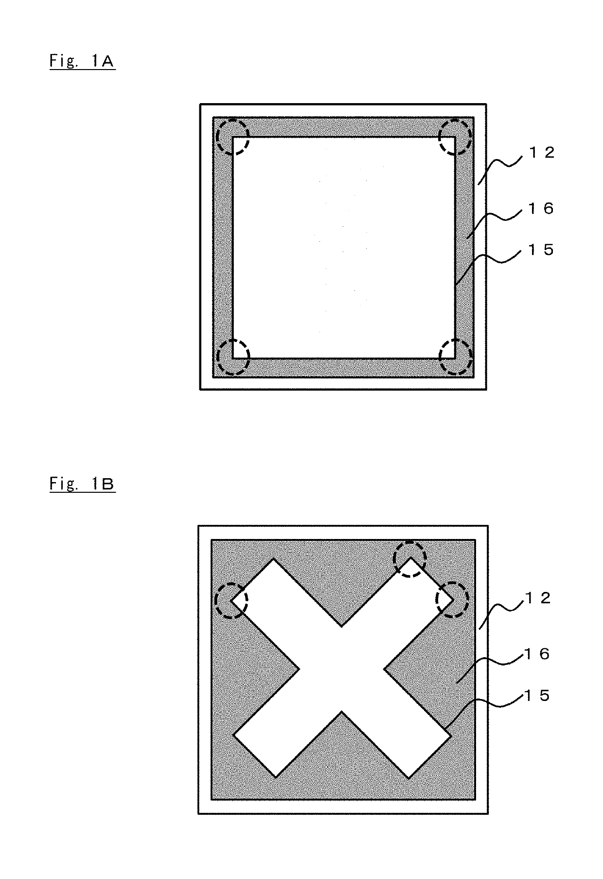
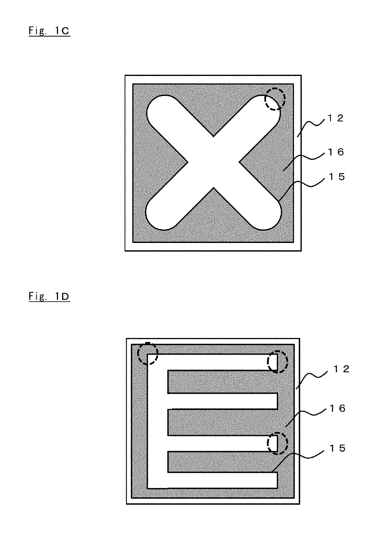
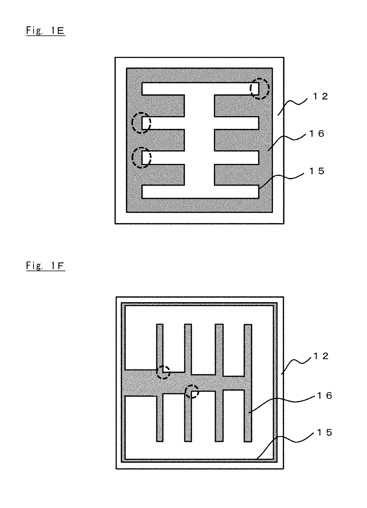
[0149]Note that, as similar to the method of Example 1, four types of elements comprising the p-electrode restricted area were made so that the distance (a) from the mesa edge of the projection part to the p-electrode were 20 μm (Example 3), 12 μm (Example 4), 8 μm (Comparative example 3) and 5 μm (Comparative example 4). Further, the distance between mesa edge and the p-electrode in the p-electrode allowed area was 5 μm. For each examples and comparative examples as mentioned in above, 50 elements were produced, and for the obtained luminescence elements, the output characteristics over the time were measured.
[0150]In the luminescence element of Example 3, the instantaneous deterioration rate (the ratio of the element having significant drop of the ...
PUM
 Abstract
Description
Claims
Application Information


