Systems, methods, and computer-readable media utilizing improved data structures and design flow for programmable memory built-in self-test (PMBIST)

a programmable memory and self-testing technology, applied in the field of integrated circuit design and testability, can solve the problems of reduced soc yield due to embedded memory, increased potential faults or defects, and reduced soc yield, etc., to facilitate more robust analysis of design requirements.

Active Publication Date: 2019-08-20
CADENCE DESIGN SYST INC
View PDF10 Cites 1 Cited by
  • Summary
  • Abstract
  • Description
  • Claims
  • Application Information

AI Technical Summary

Benefits of technology

[0009]Accordingly, to address at least some of such issues and / or problems, certain exemplary embodiments of computer systems, methods, and computer-readable media for EDA disclosed herein can utilize package files to facilitate more robust analysis of the design requirements and enable reuse of PMBIST hardware and / or clustering of memories where feasible, optimal, necessary, and / or desirable. Furthermore, such exemplary embodiments can provide an improved method, procedure, and / or design flow for PMBIST hardware insertion into an SoC design based on a “suspend / resume” feature. If errors are detected, rather than waiting for a new revision of the EDA tools that corrects the detected errors, the improved method, procedure, and / or design flow suspends the PMBIST hardware insertion until corrected package file(s) are received, then resumes the design flow based on the corrected file(s). As such, exemplary embodiments of computer systems, methods, and computer-readable media disclosed herein can vastly out-perform conventional methods, techniques, and systems in various known applications, including exemplary applications discussed herein.

Problems solved by technology

The smaller feature size and increasing portion of an SoC occupied by memories also can result in an increase in potential faults or defects and, consequently, a reduction in SoC yield due to the embedded memories.
In the context of these larger SoC designs with more memory, the conventional approach of Direct Memory Access (DMA) for memory testing can be costly in terms of silicon area, routing complexity, and test time.
Due to optimizations for cost, size, etc., such controllers conventionally have been non-programmable such that their algorithms and targeted fault models cannot be changed after the chip has been manufactured.
In addition, it can be difficult to predict all types of defects that can manifest themselves during a manufacturing process, so a designer can modify the test algorithms as these become more familiar.
A certain test suite that was effective and / or efficient for a particular technology when the SoC was originally designed may be unsatisfactory when the SoC design is migrated to a newer technology.
Several issues and / or problems can arise during the development and / or configuration of PMBIST hardware for an SoC design.
This variety of memory types and models makes early development and / or configuration of comprehensive PMBIST difficult.
In addition, the design flow in the electronic design automation (EDA) tool used for PMBIST insertion into the SoC design can be interrupted due to errors in the memory models or the tool itself, causing delay in the PMBIST hardware and, consequently, the software that is dependent on the hardware design.

Method used


Image

  • Systems, methods, and computer-readable media utilizing improved data structures and design flow for programmable memory built-in self-test (PMBIST)
  • Systems, methods, and computer-readable media utilizing improved data structures and design flow for programmable memory built-in self-test (PMBIST)
  • Systems, methods, and computer-readable media utilizing improved data structures and design flow for programmable memory built-in self-test (PMBIST)

Examples


Embodiment Construction

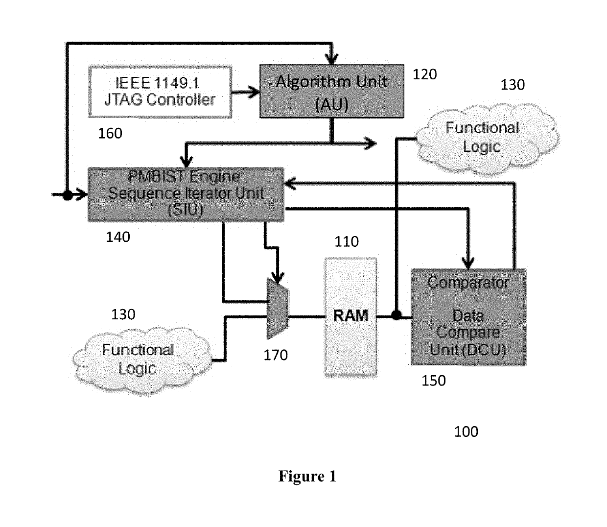
[0020]FIG. 1 is a block diagram of an exemplary PMBIST system 100 that can be utilized, for example, in an SoC design. System 100 can comprise a random access memory (RAM) 110, which is an exemplary SoC memory device to which a designer wishes to apply PMBIST principles and / or techniques described herein. As discussed above, an exemplary SOC design can comprise a plurality of memory devices such as RAM 110. System 100 can also comprise a variety of functional logic blocks 130 that can constitute the digital logic functionality of the SoC. Although two blocks 130 are shown, this is only to illustrate both input and output relationships with RAM 110, as the skilled person will readily comprehend.

[0021]System 100 can further comprise an algorithm unit (AU) 120, which embodies various PMBIST algorithms for execution by the PMBIST engine, which is illustrated as sequence iterator unit (SIU) 140. In some exemplary embodiments, AU 120 can comprise any type of readable and rewritable memory...


PUM


Abstract

Computer system for programmable built-in self-test (PMBIST) insertion into system-on-chip designs comprising one or more memories, including at least one processor and computer-executable instructions that cause the system to determine a PMBIST configuration based on one or more test configuration files; generate one or more package files based on the PMBIST configuration; insert PMBIST hardware into the SoC design based on the package files and characteristics of the memories; suspend PMBIST hardware insertion after an event related to the package files; and resume PMBIST hardware insertion after receiving one or more updated package files. In some embodiments, the package files are independent of vendor-specific memory models. In some embodiments, the package files comprise a plurality of data structures. Exemplary methods and computer-readable media can also be provided embodying one or more procedures the system is configured to perform.

Description

FIELD OF THE DISCLOSURE[0001]The present disclosure relates generally to the design of integrated circuits for testability. More specifically, the present disclosure relates to systems, methods, and computer-readable media that facilitate development of programmable memory built-in-self-test (PMBIST) by improved data structures and design flows.BACKGROUND INFORMATION[0002]A system-on-chip (SoC) is an integrated circuit that integrates various components of a computer or other electronic system fabricated on a single die (e.g., silicon die). An SoC can include digital, analog, mixed-signal, and even radio-frequency functions on a single die. SoC digital circuits can include both standard and custom logic circuits (e.g., processors), as well as memory circuits. SoCs can also include digital circuits dedicated to testing and / or verifying the functionality of other portions of the SoC, commonly known as built-in self-test (BIST).[0003]The density and / or feature size of the memories bein...

Claims


Application Information

Patent Timeline
Patent Type & Authority Patents(United States)
IPC IPC(8): G06F17/50G11C29/12G01R31/3187G06F11/27
CPCG06F17/5045G01R31/3187G06F11/27G06F17/5072G11C29/12G06F30/39G06F2115/02G11C29/16G06F30/30G06F30/392
Inventor ARORA, PUNEETGREGOR, STEVEN LEECARD, NORMAN ROBERT
Owner CADENCE DESIGN SYST INC
Why Eureka
Try Eureka