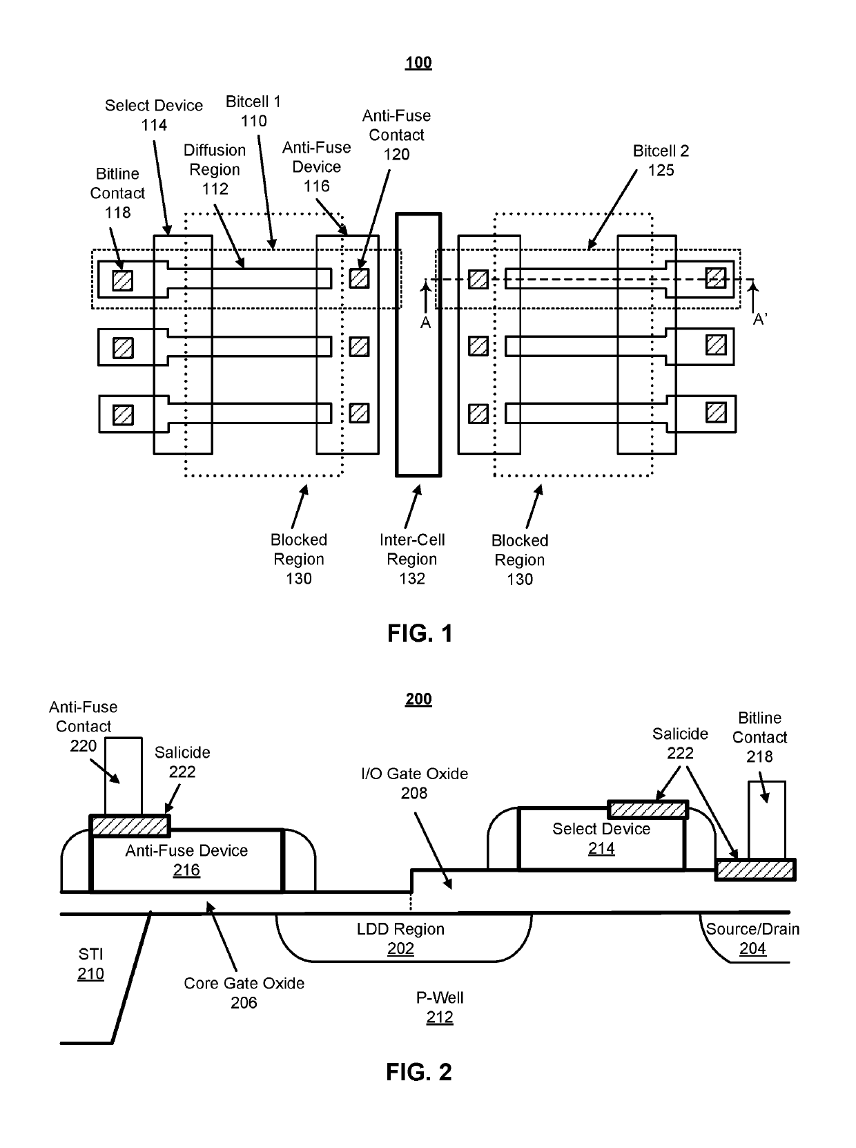
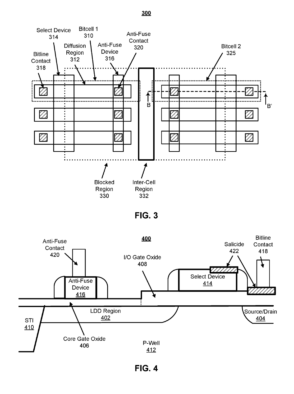
One-time programmable bitcell with native anti-fuse
a bitcell and anti-fuse technology, applied in the field of one-time programmable bitcells, can solve the problems of increasing the cost of producing bitcells, changing the performance or characteristics of produced devices, and a significant portion of the total manufacturing cost of testing time, so as to achieve the effect of increasing the breakdown voltag
- Summary
- Abstract
- Description
- Claims
- Application Information
AI Technical Summary
Benefits of technology
Problems solved by technology
Method used
Image


Examples
example table
of Operations
[0052]FIG. 8 is a table of operation voltages of an OTP memory device according to one embodiment. The table of operation provides the voltage levels at different points in a memory device (given along the top of the table) and for different operations (given along the left side of the table). Vrupt is the high voltage used to rupture the gate oxide when a bitcell is being programmed. VDD refers to the power supply voltage for the core logic device, such as 1.8V in a 1.8V / 5V process. VDD_IO refers to the power supply voltage for the 10 logic device, such as 5V in a 1.8V / 5V process.
Overview of Electronic Design Automation Design Flow
[0053]FIG. 9 is a flowchart 900 illustrating the various operations in the design and fabrication of an integrated circuit. This process starts with the generation of a product idea 910, which is realized during a design process that uses electronic design automation (EDA) software 912. When the design is finalized, it can be taped-out 934. A...
PUM
 Abstract
Description
Claims
Application Information