Method for manufacturing thin film transistor substrate

a manufacturing method and technology of transistors, applied in the direction of electrical equipment, semiconductor devices, instruments, etc., can solve the problems of difficulty in attaining the required positional accuracy and actualizing the required accuracy, and achieve the effect of reducing the variation of positional accuracy

Inactive Publication Date: 2019-08-27
SAKAI DISPLAY PROD
View PDF15 Cites 2 Cited by
  • Summary
  • Abstract
  • Description
  • Claims
  • Application Information

AI Technical Summary

Benefits of technology

[0024]The present invention has been made in view of the above circumstances, and an object of the present invention is to provide a manufacturing method for a thin-film transistor substrate, which enables to excellently perform alignment between an annealed region of a semiconductor film and a pattern of a conductive film, thereby a satisfactory positional accuracy between the annealed region and source line, for example, is attained and variations in positional accuracy can be reduced between TFTs.

Problems solved by technology

However, since positions are not directly adjusted between the annealed portion and the photomask 60 for the conductive film (source film), it is difficult to attain a required positional accuracy.
In the case where a process is performed by using a mask which is completely different in size from a mask for exposure of a predetermined pattern, and a high positional accuracy between them is needed, it is considered difficult for the technique disclosed in No. 2012-119680 to actualize the required accuracy.

Method used


Image

  • Method for manufacturing thin film transistor substrate
  • Method for manufacturing thin film transistor substrate
  • Method for manufacturing thin film transistor substrate

Examples


embodiment 1

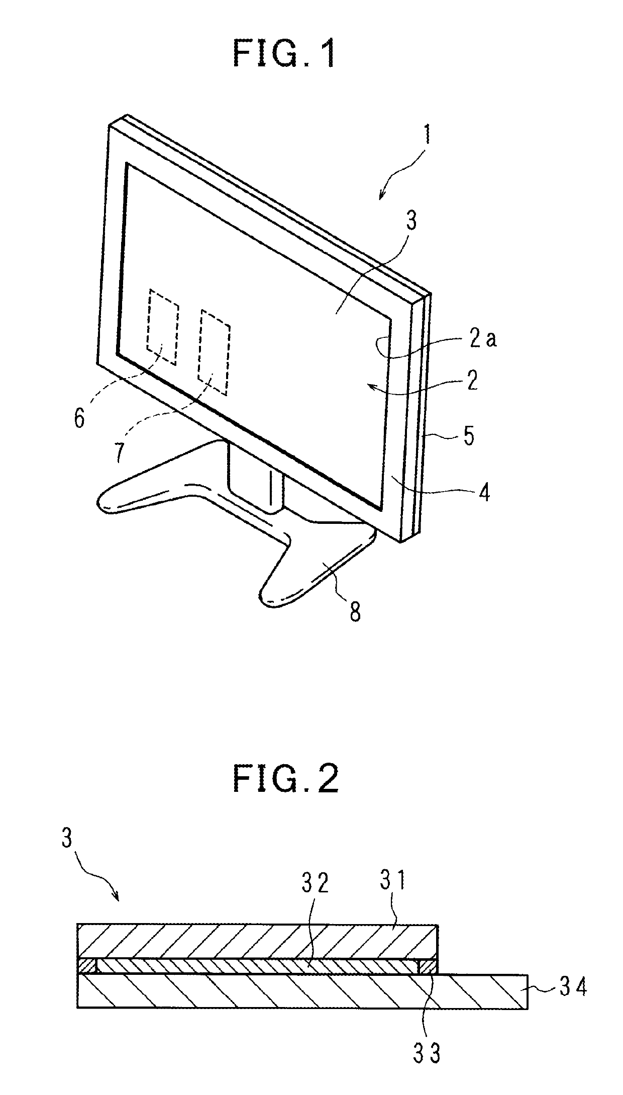
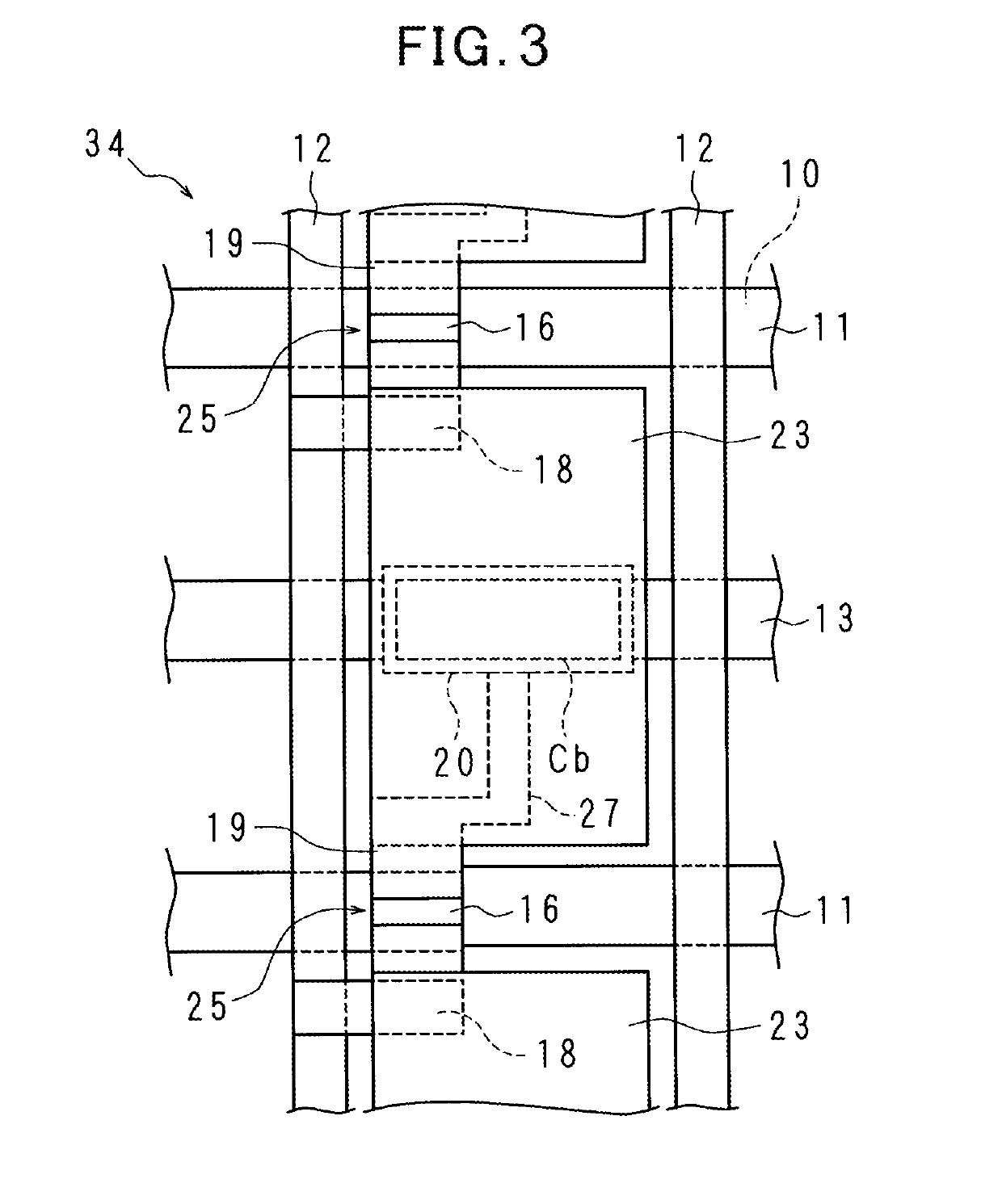
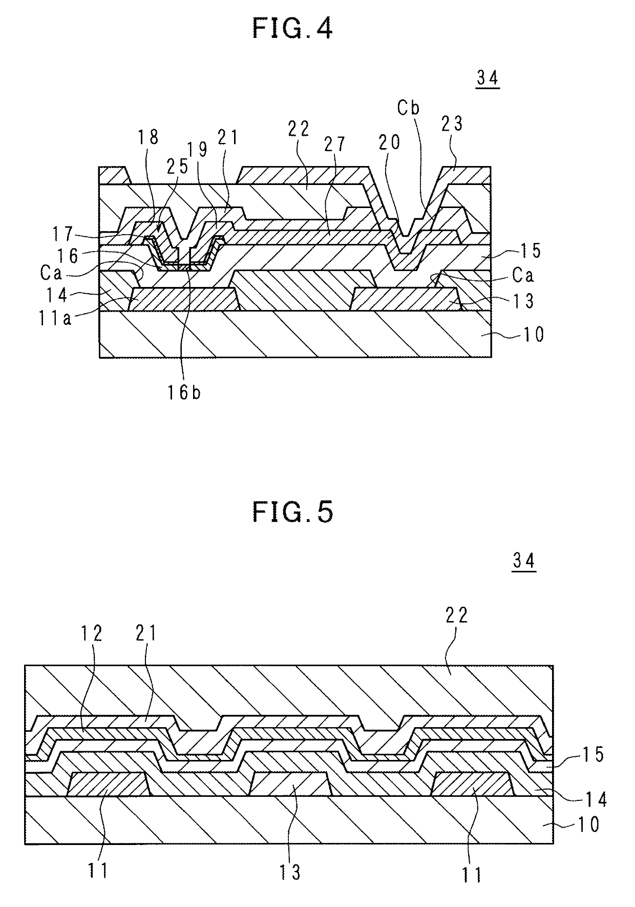
[0045]FIG. 1 shows a schematic perspective view of the TV receiver 1 according to Embodiment 1, FIG. 2 shows a schematic cross-sectional view of a display panel 3 according to Embodiment 1, FIG. 3 shows a schematic plan view of pixels on a TFT substrate 34 according to Embodiment 1, FIG. 4 shows a schematic cross-sectional view of a portion of the TFT substrate 34 according to Embodiment 1, in which a TFT 25 is arranged, and FIG. 5 shows a schematic cross-sectional view of a portion of the TFT substrate 34 according to Embodiment 1, in which a source line 12 and gate line 11 cross.

[0046]The TV receiver 1 includes a horizontally long display module 2 with which to display an image, a tuner 6 with which to receive a broadcast wave from an antenna (not shown), and a decoder 7 with which to decode an encoded broadcast wave. The TV receiver 1 may display an image on the display module 2 according to decoded information output by the decoder 7, which decodes the broadcast wave received by...

embodiment 2

[0088]FIG. 13 shows a schematic plan view of the positional relationship among the mother glass substrate 70, the TFT array region 30, the first alignment mark 71, and the photomask 60. FIG. 13 shows an exemplary embodiment in which the TFT array regions 30 are formed in plurality such that the longitudinal direction of the TFT array region 30 is positioned perpendicular to the longitudinal direction of the mother glass substrate 70, and each of the TFT array regions 30 is cut out from the mother glass substrate 70. It should be noted that the TFT array region 30 is omitted in the magnified view according to FIG. 13.

[0089]In the exemplary embodiment shown in FIG. 13, the direction of the longitudinal direction of the TFT array region 30 with respect to the longitudinal direction of the mother glass substrate 70 is rotated by 90 degrees from the direction of the longitudinal direction of the TFT array region 30 with respect to the longitudinal direction of the mother glass substrate ...

embodiment 3

[0094]A manufacturing method for the TFT array region 30 according to Embodiment 3 is different from the manufacturing methods for the TFT array region 30 according to Embodiments 1 and 2 in that an alignment mark (a second alignment mark) 26 is formed on the basis of a first alignment mark 71.

[0095]FIG. 14 shows a flow chart indicating a manufacturing method for a TFT substrate 30 according to Embodiment 3, and FIG. 15 shows a schematic plan view of a relationship between a mask 50 and a photomask 60. An exemplary embodiment in which a TFT array region 30 having a similar structure to the TFT array region 30 according to Embodiment 1 is manufactured will be described below. As with Embodiment 1, the interlayer insulation film 14 may not be formed.

[0096]First, a metal film is formed over the entire surface of an insulation substrate 10 such as a glass substrate by sputtering, and then a gate line 11 (including a gate electrode 11a) and a capacitor line 13 are formed by photolithogra...


PUM

PropertyMeasurementUnit
conductiveaaaaaaaaaa
lengthaaaaaaaaaa
energyaaaaaaaaaa

Abstract

There is provided a manufacturing method for a thin-film transistor substrate, which enables to excellently perform alignment between an annealed region of a semiconductor film and a mask pattern of a conductive film. The method comprises annealing a semiconductor film being formed on a gate insulation film covering a gate electrode with a laser beam by using a mask, the gate electrode being formed within a thin-film transistor substrate region on a substrate; forming a first alignment mark outside the thin-film transistor substrate region on the substrate, by irradiating the substrate through the mask with the laser beam; patterning the semiconductor film; forming a conductive film on the semiconductor film; positioning a photomask on the basis of the first alignment mark; and forming a source electrode and a drain electrode by patterning the conductive film through the photomask; wherein the first alignment mark is formed while annealing the semiconductor film.

Description

CROSS-REFERENCE TO RELATED APPLICATION[0001]This is a continuation-in-part of PCT international application No. PCT / JP2015 / 080617 filed on Oct. 29, 2015, incorporated herein by reference.TECHNICAL FIELD[0002]The present invention relates to a manufacturing method for a thin-film transistor substrate (hereinafter referred to as a TFT substrate) provided in display apparatus for, for example, a television receiver, a personal computers.BACKGROUND OF THE INVENTION[0003]Within the field of the display apparatus, a liquid crystal display apparatus can have characteristics of thin profile and low power consumption. A liquid crystal display apparatus provided with a TFT substrate, having a switching element such as thin-film transistor (TFT) at each pixel, especially has a high contrast ratio and excellent response characteristics and exhibits high performance. Therefore, it is suitably used for, for example, a television receiver, a personal computer.[0004]A plurality of gate lines (scan ...

Claims


Application Information

Patent Timeline
Patent Type & Authority Patents(United States)
IPC IPC(8): H01L29/786H01L27/12G02F1/1362G02F1/1335G02F1/1333G02F1/1368
CPCH01L27/1285H01L27/1288G02F1/1368G02F1/133354H01L29/786G02F1/133345G02F1/133514G02F1/136286G02F2201/123H01L27/124
Inventor KATO, MASAHIRO
Owner SAKAI DISPLAY PROD
Why Eureka
Try Eureka