

Wiring board desmear treatment method
a treatment method and wiring board technology, applied in the field of desmear treatment of wiring boards, can solve the problems of excessive roughness fall of wiring and deterioration of the responsiveness of high-frequency signals, and further roughening of the surface of the insulating layer
- Summary
- Abstract
- Description
- Claims
- Application Information
AI Technical Summary
Benefits of technology
Problems solved by technology
Method used
Image

Examples
example 1
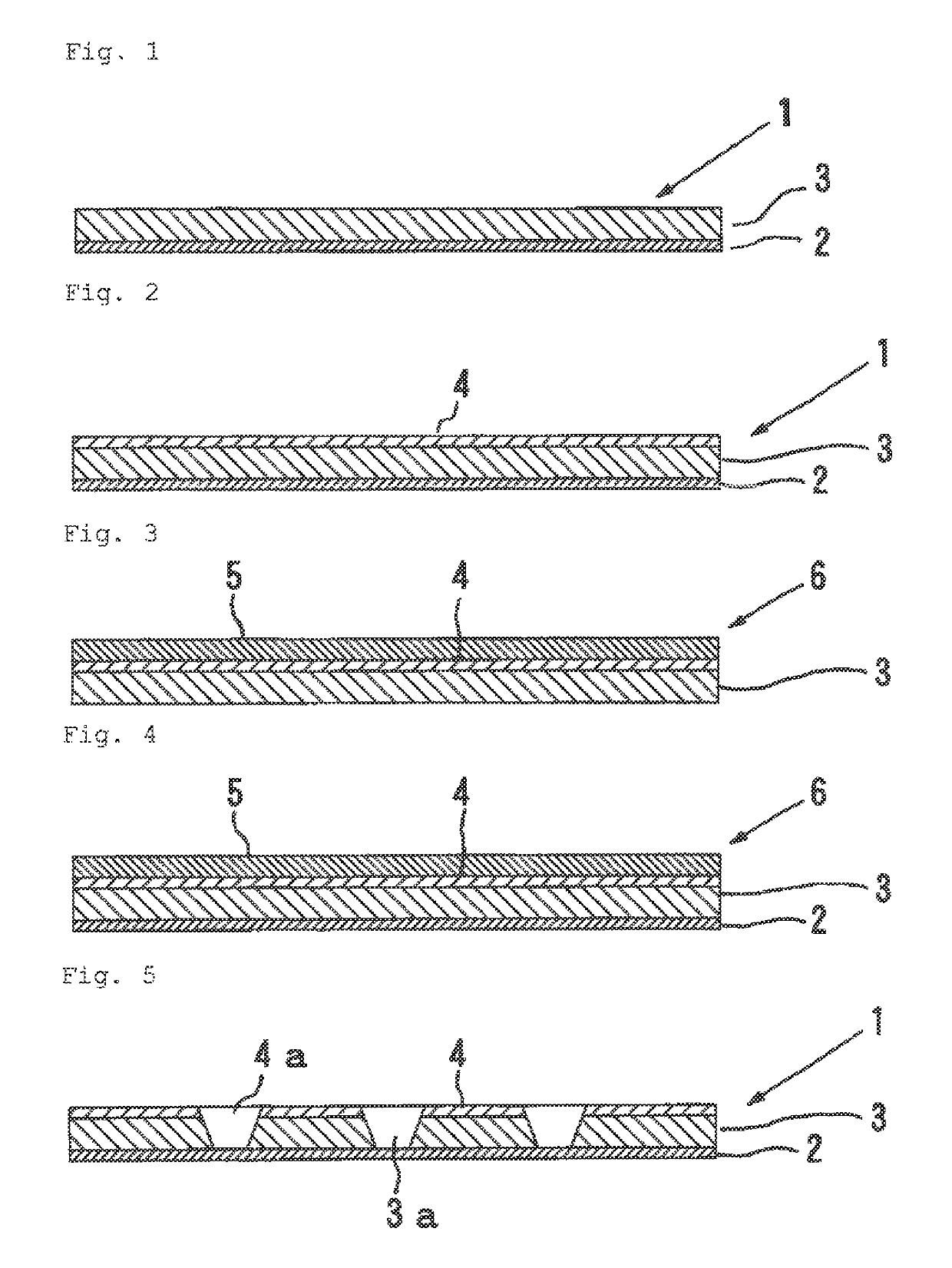
(1) Manufacture of Wiring Board Material
[0090]A copper-clad laminate in which copper foil was layered on a surface of an insulating substrate to have a thickness of 0.4 mm was prepared. The copper foil in the copper-clad laminate was subjected to photolithography and etching to form a conductive layer having a required pattern on the surface of the insulating substrate.
[0091]An insulating film (“ABF-GX92” manufactured by Ajinomoto Fine-Techno Co., Inc.) in which an insulating layer containing a filler was layered on a PET film, which was a carrier layer, was laminated on the surface of the insulating substrate including the conductive layer. After that, the PET film was peeled off. The thickness of the insulating layer in this insulating film was 20 μm. Such lamination was performed with a batch-type vacuum pressure laminator at an atmospheric pressure not more than 10,000 hPa under conditions of a temperature of 110° C. and a pressure of 500 kN / m2. After that, the insulating layer ...
example 2
(1) Manufacture of Composite Insulating Layer Forming Material
[0110]Twenty parts by mass of a liquid bisphenol A epoxy resin (“jER@ 828EL” manufactured by Mitsubishi Chemical Corporation), 12 parts by mass of an epoxy resin curing agent (“jER@ cure ST12” manufactured by Mitsubishi Chemical Corporation) and a diluent (“reactive diluent YDE” manufactured by Mitsubishi Chemical Corporation) were mixed together to prepare a coating liquid for forming a depletable resist layer.
[0111]The coating liquid for forming a depletable resist layer was applied, with a die coater, to a base layer made of a PET film (manufactured by Lintec Corporation, a thickness of 38 μm) with an alkyd-type parting agent (AL-5). The coated liquid was subjected to a drying treatment at 100° C. for 5 minutes to form a depletable resist layer made of the epoxy resin and having a thickness of 1.5 μm on the base layer.
[0112]Next, 28 parts by mass of a liquid bisphenol A epoxy resin (“jER@ 828EL” manufactured by Mitsubi...
PUM
| Property | Measurement | Unit |
|---|---|---|
| wavelength | aaaaa | aaaaa |
| thickness | aaaaa | aaaaa |
| wavelength | aaaaa | aaaaa |
Abstract
Description
Claims
Application Information