
Photomask blank, and preparation method thereof

a technology of photomask and blank, applied in the field of photomask, can solve the problems of volume change, defect generation, and defect generation, and achieve the effect of reducing volume and reducing production costs

Active Publication Date: 2020-02-18
SHIN ETSU CHEM IND CO LTD
View PDF8 Cites 3 Cited by
  • Summary
  • Abstract
  • Description
  • Claims
  • Application Information

AI Technical Summary

Benefits of technology

The patent text describes a way to make a photomask with two layers - one containing chromium and one containing silicon. By combining these layers, the photomask is less likely to have defects and become less effective over time. This helps ensure consistent and reliable performance of the photomask during use.

Problems solved by technology

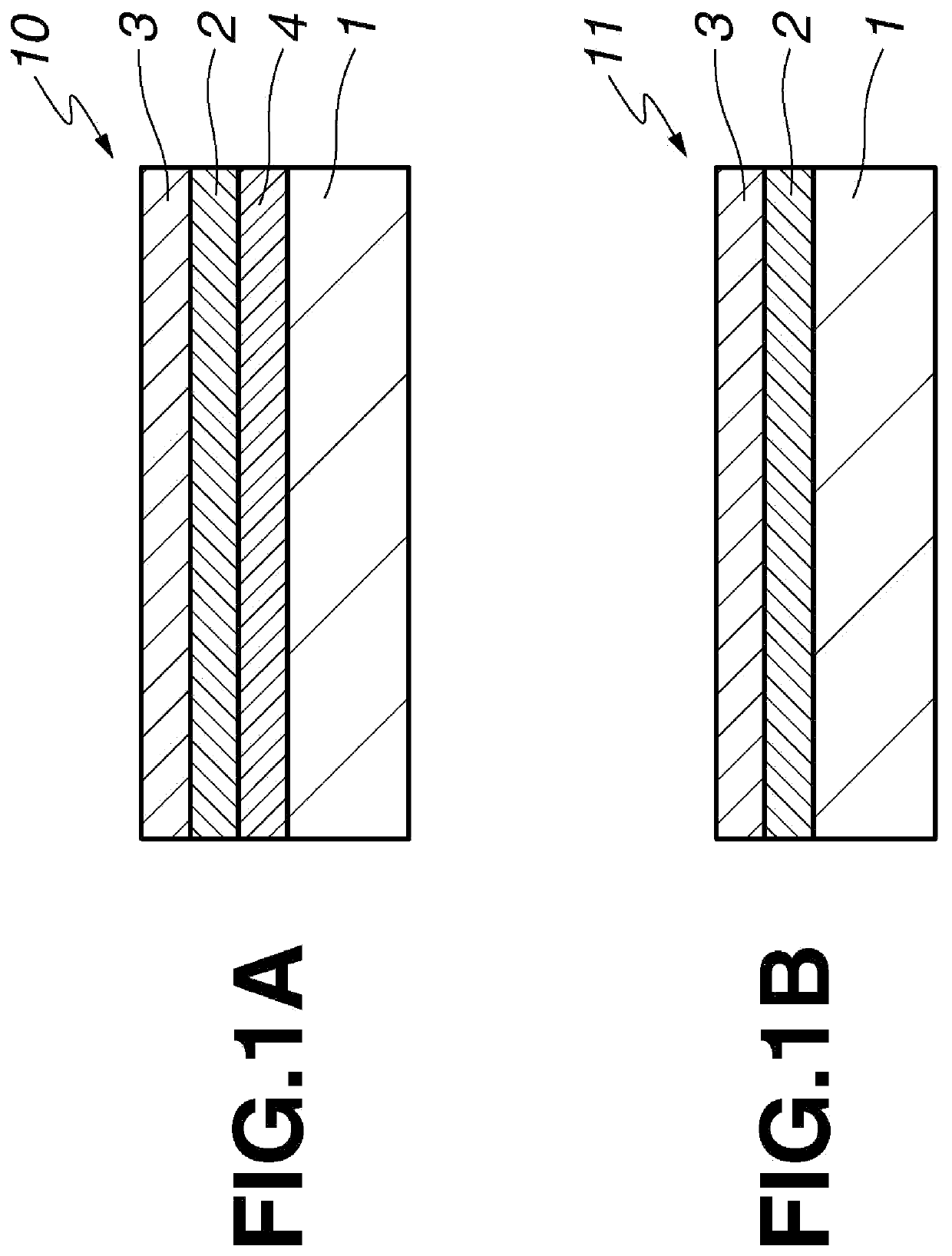
However, it was found that defects are generated due to deterioration with age when a photomask blank or photomask has a film structure including a chromium-containing film and a silicon-containing film contacted to each other.
The defects are resulted with volume change caused by oxidation of chromium contained in the film containing chromium and nitrogen with oxygen contained in the film containing silicon and oxygen at the interface or its vicinity of the film containing chromium and nitrogen and the film containing silicon and oxygen.

Method used


Image

  • Photomask blank, and preparation method thereof
  • Photomask blank, and preparation method thereof
  • Photomask blank, and preparation method thereof

Examples


example 1

[0066]A phase shift film of MoSiON (75 nm thick) was formed on a quartz substrate of 154 mm square×about 6.35 mm thick by a sputtering method. Oxygen, nitrogen and argon gases were used as sputtering gas. Two kinds of MoSi2 target and Si target were used as targets. While the substrate was rotated on its axis of rotation at 30 rpm, the film was deposited. The composition of the film was analyzed by EPMA utilizing XPS (x-ray photoelectron spectroscopy) system (Thermo Fisher Scientific Inc., K-Alpha), and was Mo:Si:O:N=1:4:1:4 (atomic ratio).

[0067]Next, as the film (A), a light-shielding film consisting of two layers of a CrN layer (30 nm thick) and a CrON layer (20 nm thick) disposed in the order from substrate side was formed on the phase shift film by a sputtering method. Nitrogen and argon gases (CrN layer) and oxygen, nitrogen and argon gases (CrON layer) were used as sputtering gases, respectively. Chromium metal target was used as a target. While the substrate was rotated on it...

example 2

[0071]A phase shift film and film (A) was formed on a quartz substrate by the same manner as shown in Example 1. Next, as the film (B), a hard mask film of single layer (5 nm thick) composed of SiO was formed on the film (A) by a sputtering method. Oxygen and argon gases were used as sputtering gas. Si target was used as a target. While the substrate was rotated on its axis of rotation at 30 rpm, the film was deposited. A flow rate of argon and a power applied across the target were set as same as Example 1. In this case, while 1 / 20 of the whole time for depositing of the hard mask from the start of the spattering, oxygen gas was same, thereafter, oxygen gas was set to lower flow rate of 20 sccm. The composition of the film was analyzed by EPMA, and was Si:O=1:1.2 (atomic ratio) in the whole of the film.

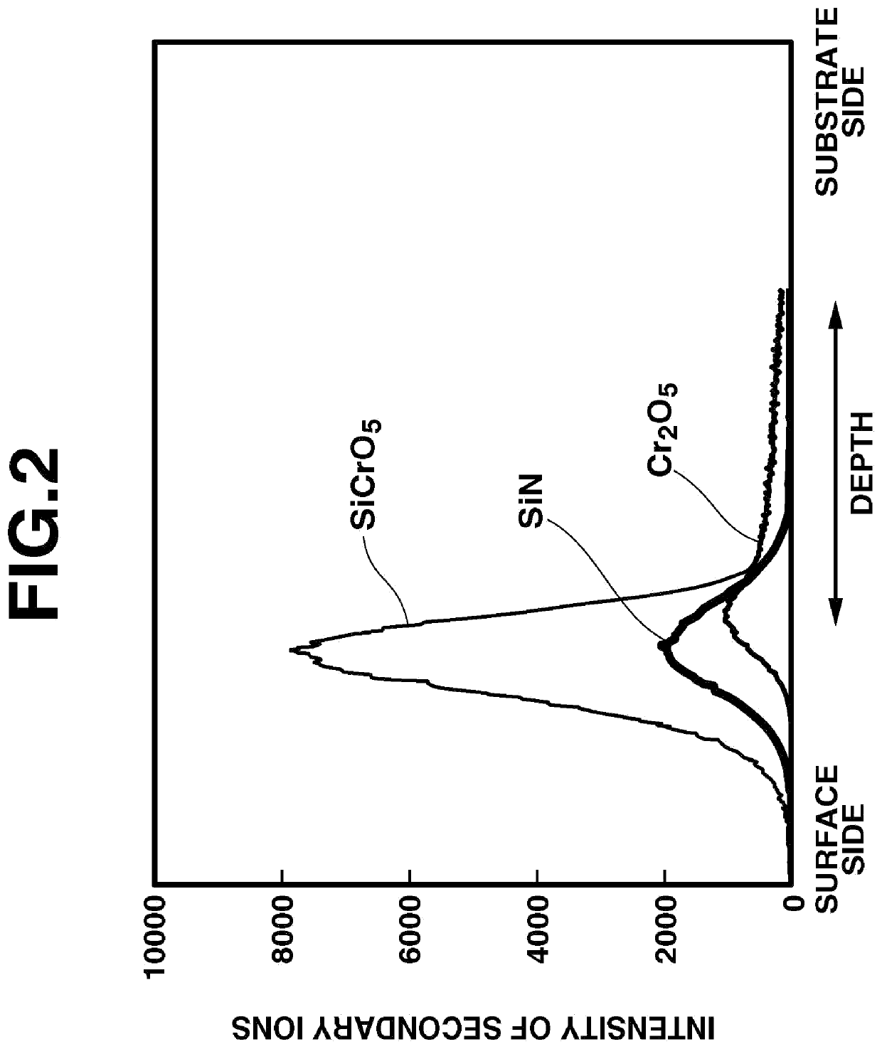
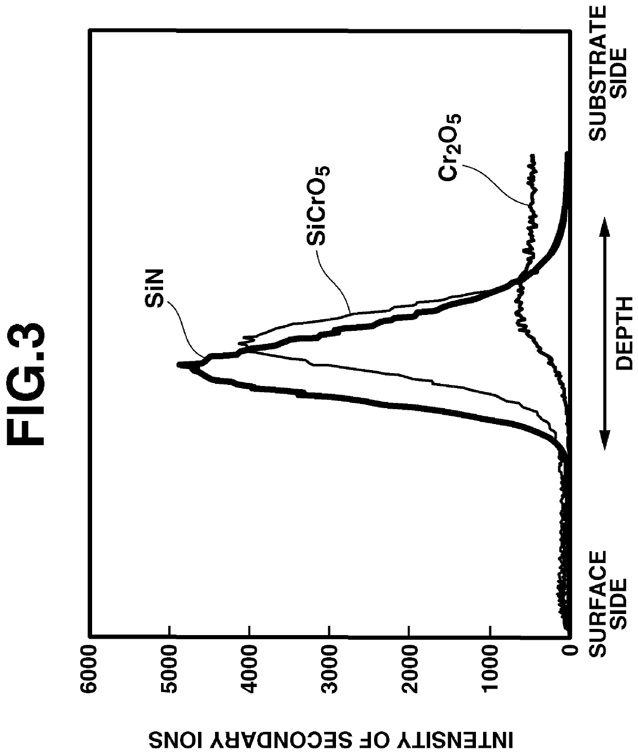
[0072]Intension distributions of several kinds of emitted secondary ions were measured at a position located at the interface or its vicinity of the film (A) and film (B) by the same...


PUM

PropertyMeasurementUnit
thicknessaaaaaaaaaa
thicknessaaaaaaaaaa
thicknessaaaaaaaaaa

Abstract

A photomask blank including a transparent substrate, and at least one film (A) containing chromium and nitrogen and free of silicon and at least one film (B) containing silicon and oxygen, and free of a transition metal that are contacted to each other In the blank, when an intension of secondary ions is measured along a thickness direction of the films by a time-of-flight secondary ion mass spectrometry (TOF-SIMS), an intension of secondary ions derived from Cr2O5 is lower than an intension of secondary ions derived from SiN, at a position located at the interface or its vicinity of the film (A) and film (B) and having a maximum intensity of secondary ions derived from SiCrO5.

Description

CROSS-REFERENCE TO RELATED APPLICATION[0001]This non-provisional application claims priority under 35 U.S.C. § 119(a) on Patent Application No. 2016-250722 filed in Japan on Dec. 26, 2016, the entire contents of which are hereby incorporated by reference.TECHNICAL FIELD[0002]This invention relates to a photomask blank which is processed into a photomask for use in the microfabrication of semiconductor integrated circuits, and a method for preparing the same.BACKGROUND ART[0003]In the field of semiconductor technology, research and development efforts are continued for further miniaturization of pattern features. Recently, as advances including miniaturization of circuit patterns, thinning of interconnect patterns and miniaturization of contact hole patterns for connection between cell-constituting layers are in progress to comply with higher integration density of LSIs, there is an increasing demand for the micropatterning technology. Accordingly, in conjunction with the technology ...

Claims


Application Information

Patent Timeline
Patent Type & Authority Patents(United States)
IPC IPC(8): G03F1/32G03F1/54G03F1/84G03F1/26
CPCG03F1/26G03F1/84G03F1/32G03F1/54G03F1/00G03F1/62G03F1/68G03F1/50H01L21/02631
Inventor KOSAKA, TAKUROINAZUKI, YUKIO
Owner SHIN ETSU CHEM IND CO LTD
Learn More