Integrated circuit (IC) interconnect structure having a metal layer with asymmetric metal line-dielectric structures supporting self-aligned vertical interconnect accesses (VIAS)

a technology of integrated circuits and interconnect structures, which is applied in the direction of electrical equipment, semiconductor devices, semiconductor/solid-state device details, etc., can solve the problems of increasing the switching speed of interconnected devices, reducing device switching speed, and overall reducing device resistance, so as to facilitate interconnection, prevent metal line shorting, and increase the cross-sectional area

Active Publication Date: 2020-05-12
QUALCOMM INC
View PDF1 Cites 3 Cited by
  • Summary
  • Abstract
  • Description
  • Claims
  • Application Information

AI Technical Summary

Benefits of technology

[0005]An integrated circuit (IC) interconnect structure having a metal layer with asymmetric metal line-dielectric structures supporting self-aligned vertical interconnect accesses (vias) is disclosed. The interconnect structure comprises a plurality of metal layers, each comprising one or more metal lines spaced at a metal line pitch (e.g., center-to-center distance). The metal lines facilitate interconnections between semiconductor devices formed in the IC. The interconnect structure further comprises dielectric structures disposed between adjacent metal lines to prevent metal line shorting. In exemplary aspects disclosed herein, the width of the metal lines is asymmetric to (e.g., greater than) the width of dielectric structures between adjacent metal lines, providing an asymmetric width relationship between the metal line and its adjacent dielectric structure. This allows a metal line to have a greater cross-sectional area for reducing electrical resistance between interconnected devices without having to increase metal line pitch. Reduced electrical resistance in a metal line can result in an overall reduced device resistance, thus increasing interconnected device switching speeds.

Problems solved by technology

Reduced electrical resistance in a metal line can result in an overall reduced device resistance, thus increasing interconnected device switching speeds.
However, because a distance between the metal lines is reduced due to their wider, asymmetric widths relative to their adjacent dielectric structures, the capacitive coupling between adjacent metal lines may increase, thereby decreasing device switching speeds and potentially offsetting the positive effect of the reduced resistance of the metal lines.

Method used


Image

  • Integrated circuit (IC) interconnect structure having a metal layer with asymmetric metal line-dielectric structures supporting self-aligned vertical interconnect accesses (VIAS)
  • Integrated circuit (IC) interconnect structure having a metal layer with asymmetric metal line-dielectric structures supporting self-aligned vertical interconnect accesses (VIAS)
  • Integrated circuit (IC) interconnect structure having a metal layer with asymmetric metal line-dielectric structures supporting self-aligned vertical interconnect accesses (VIAS)

Examples


Embodiment Construction

[0028]With reference now to the drawing figures, several exemplary aspects of the present disclosure are described. The word “exemplary” is used herein to mean “serving as an example, instance, or illustration.” Any aspect described herein as “exemplary” is not necessarily to be construed as preferred or advantageous over other aspects.

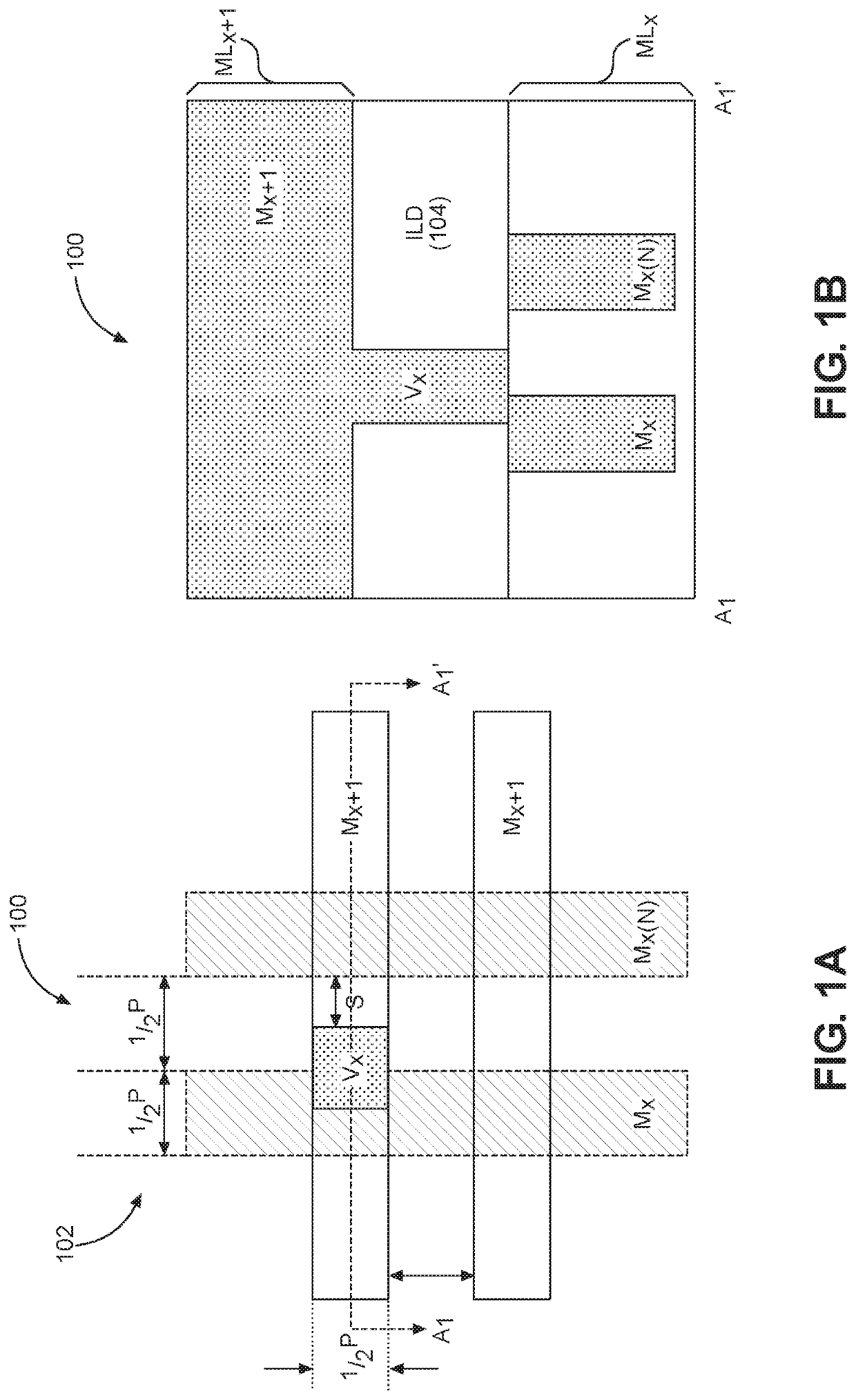
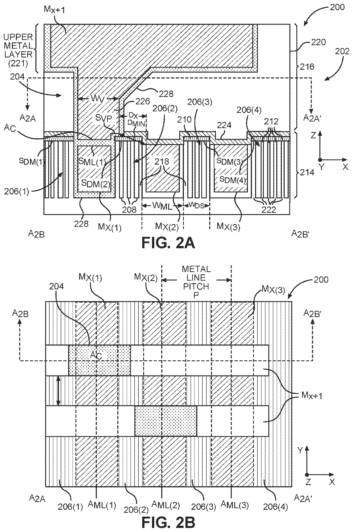
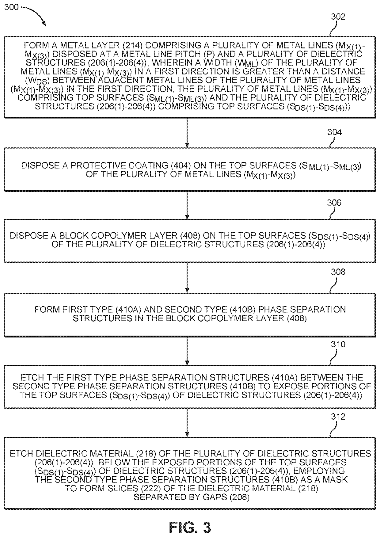
[0029]An integrated circuit (IC) interconnect structure having a metal layer with asymmetric metal line-dielectric structures supporting self-aligned vertical interconnect accesses (vias) is disclosed. The interconnect structure comprises a plurality of metal layers, each comprising one or more metal lines spaced at a metal line pitch (e.g., center-to-center distance). The metal lines facilitate interconnections between semiconductor devices formed in the IC. The interconnect structure further comprises dielectric structures disposed between adjacent metal lines to prevent metal line shorting. In exemplary aspects disclosed herein, the width of the me...


PUM

PropertyMeasurementUnit
thicknessaaaaaaaaaa
dielectric constantaaaaaaaaaa
relative permittivityaaaaaaaaaa

Abstract

An integrated circuit (IC) interconnect structure may include a metal layer with asymmetric metal line-dielectric structures supporting fully self-aligned vertical interconnect accesses (vias). The interconnect structure includes metal lines spaced at a metal line pitch and dielectric structures disposed between adjacent metal lines. The width of the metal lines is asymmetric to the width of dielectric structures, providing an asymmetric width relationship that allows a metal line to have a greater cross-sectional area for reducing electrical resistance without having to increase metal line pitch. The via pattern is self-aligned to an upper metal opening at the top and an underlayer metal recess opening at the bottom, allowing the maximum contact area to reduce via resistance. To reduce capacitive coupling between adjacent metal lines, the adjacent interconnect structures include a plurality of gaps formed in a dielectric material of the dielectric structure.

Description

BACKGROUNDI. Field of the Disclosure[0001]The technology of the disclosure relates generally to metal interconnect structures formed in integrated circuits (ICs), and more particularly to forming vertical interconnect accesses (vias) in metal interconnect structures to provide interconnections between metal lines in the metal interconnect structures.II. Background[0002]Current semiconductor fabrication of integrated circuits (ICs) may include front-end-of-line (FEOL), middle-of-line (MOL), and / or back-end-of-line (BEOL) processes. Semiconductor devices are created by the FEOL and MOL processes. The BEOL processes may include formation of gate contacts, interconnection among differing layers of the ICs, and a series of wafer processing steps for interconnecting the semiconductor devices created during the FEOL and MOL processes. Conventional BEOL processes in semiconductor fabrication employ metal (i.e., copper (Cu)) interconnect structures (“metal interconnects”) separated by dielec...

Claims


Application Information

Patent Timeline
Patent Type & Authority Patents(United States)
IPC IPC(8): H01L23/522H01L23/528H01L21/768
CPCH01L21/76897H01L23/5283H01L21/7682H01L21/76837H01L21/76802H01L21/76831H01L23/5226H01L21/76804H01L21/76807H01L21/76834
Inventor BAO, JUNJINGNALLAPATI, GIRIDHARCHIDAMBARAM, PERIANNAN
Owner QUALCOMM INC
Why Eureka
Try Eureka