Multilayer ceramic capacitor

a multi-layer ceramic and capacitor technology, applied in the field of multi-layer ceramic capacitors, can solve the problem of difficult to suppress the diffusion intrusion of hydrogen in the shape of a proton, and achieve the effect of suppressing the diffusion intrusion of hydrogen

Active Publication Date: 2020-06-02
TAIYO YUDEN KK
View PDF36 Cites 8 Cited by
  • Summary
  • Abstract
  • Description
  • Claims
  • Application Information

AI Technical Summary

Benefits of technology

[0006]The present invention has a purpose of providing a multilayer ceramic capacitor that is capable of suppressing diffusion intrusion of a hydrogen in a shape of a proton.

Problems solved by technology

However, with the above-mentioned technologies, it is difficult to suppress diffusion intrusion of a hydrogen in a shape of a proton.

Method used


Image

  • Multilayer ceramic capacitor
  • Multilayer ceramic capacitor
  • Multilayer ceramic capacitor

Examples


embodiment

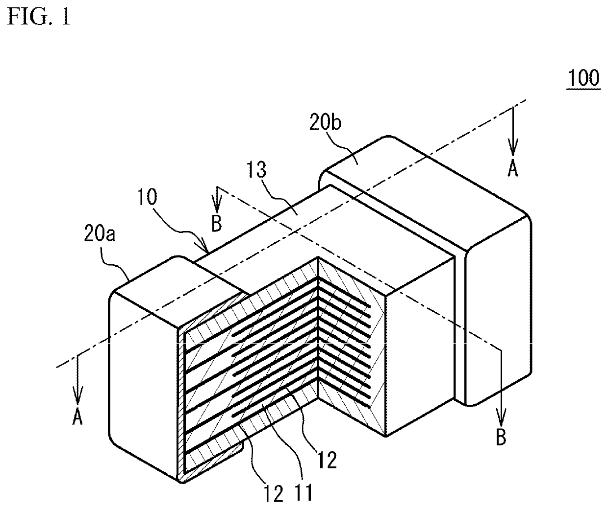
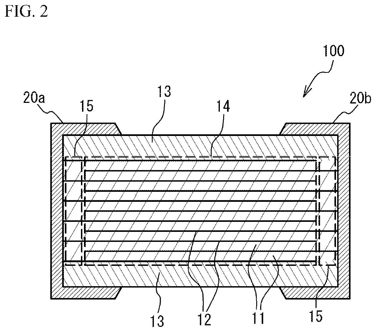
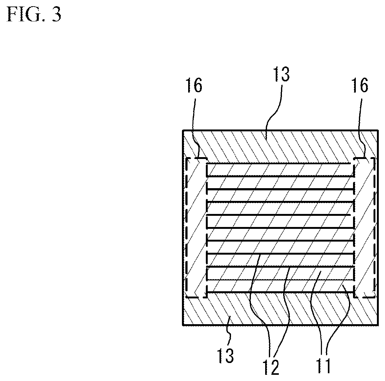
[0017]FIG. 1 illustrates a partial perspective view of a multilayer ceramic capacitor 100 in accordance with an embodiment. FIG. 2 illustrates a cross sectional view taken along a line A-A of FIG. 1. FIG. 3 illustrates a cross sectional view taken along a line B-B of FIG. 1. As illustrated in FIG. 1 to FIG. 3, the multilayer ceramic capacitor 100 includes a multilayer chip 10 having a rectangular parallelepiped shape, and a pair of external electrodes 20a and 20b that are respectively provided at two edge faces of the multilayer chip 10 facing each other. In four faces other than the two edge faces of the multilayer chip 10, two faces other than an upper face and a lower face of the multilayer chip 10 in a stacking direction are referred to as side faces. The external electrodes 20a and 20b extend to the upper face, the lower face and the two side faces of the multilayer chip 10. However, the external electrodes 20a and 20b are spaced from each other.

[0018]The multilayer chip 10 has...

first modified embodiment

[0040]Next, a description will be given of a manufacturing method for forming the protective region 17 in the end margin 15. The manufacturing method is different from the above-mentioned method only in the stacking process. Therefore, a description will be given of the different point. A binder such as polyvinyl butyral (PVB) resin, an organic solvent such as ethanol or toluene, and a plasticizer such as dioctyl phthalate (DOP) are added to the resulting ceramic material powder and wet-blended. With use of the resulting slurry, a strip-shaped dielectric green sheet with a thickness of 0.8 μm or less is coated on a base material by, for example, a die coater method or a doctor blade method, and then dried.

[0041]Then, a pattern of the internal electrode layer 12 is provided on the surface of the dielectric green sheet by printing a conductive paste for forming the internal electrode with use of screen printing or gravure printing. The conductive paste includes a powder of the main co...

second modified embodiment

[0046]Next, a description will be given of a manufacturing method for forming the protective region 17 in the side margin 16. A description will be given of the stacking process, as well as the first modified embodiment. A binder such as polyvinyl butyral (PVB) resin, an organic solvent such as ethanol or toluene, and a plasticizer such as dioctyl phthalate (DOP) are added to the resulting ceramic material powder obtained in the making process and wet-blended. With use of the resulting slurry, a strip-shaped dielectric green sheet with a thickness of 0.8 μm or less is coated on a base material by, for example, a die coater method or a doctor blade method, and then dried.

[0047]Then, a pattern of the internal electrode layer 12 is provided on the surface of the dielectric green sheet by printing a conductive paste for forming the internal electrode with use of screen printing or gravure printing. The conductive paste includes a powder of the main component metal of the internal electr...


PUM

PropertyMeasurementUnit
thicknessaaaaaaaaaa
grain diameteraaaaaaaaaa
heightaaaaaaaaaa

Abstract

A multilayer ceramic capacitor includes: a multilayer structure in which each of ceramic dielectric layers and each of internal electrode layers are alternately stacked, the plurality of internal electrode layers being alternately exposed to a first edge face and a second edge face of the multilayer structure, wherein: a region in which a set of internal electrode layers exposed to the first edge face of the multilayer structure face with another set of internal electrode layers exposed to the second edge face of the multilayer structure is a capacity region; at least a part of the circumference region around the capacity region has a protective region of which an average grain diameter of a main component ceramic is larger than that of the capacity region and of which a concentration of a donor element in the main component ceramic is larger than that of the capacity region.

Description

CROSS-REFERENCE TO RELATED APPLICATION[0001]This application is based upon and claims the benefit of priority of the prior Japanese Patent Application No. 2017-029615, filed on Feb. 21, 2017, the entire contents of which are incorporated herein by reference.FIELD[0002]A certain aspect of the present invention relates to a multilayer ceramic capacitor.BACKGROUND[0003]A multilayer ceramic capacitor has a multilayer structure in which dielectric layers and internal electrode layers are alternately stacked, and a pair of external electrodes that are formed on a surface of the multilayer structure and are electrically coupled to the internal electrodes that are extracted to the surface of the multilayer structure. A hydrogen may enter the multilayer structure in a plating process of the external electrodes or in a high temperature and high humidity condition. This causes proton conduction. And, degradation of insulating property may occur in the multilayer ceramic capacitor.[0004]And so,...

Claims


Application Information

Patent Timeline
Patent Type & Authority Patents(United States)
IPC IPC(8): H01G4/30H01G4/002H01G4/12H01G4/232H01G4/224H01G4/248H01G4/012
CPCH01G4/1227H01G4/002H01G4/12H01G4/224H01G4/30H01G4/232H01G4/248H01G4/012H01G13/00H01G13/003H01G4/1209
Inventor MORITA, KOICHIRO
Owner TAIYO YUDEN KK
Why Eureka
Try Eureka