Supercharge Your Innovation With Domain-Expert AI Agents!

Light emitting diode apparatus and manufacturing method thereof

a technology of light-emitting diodes and led apparatus, which is applied in the direction of electrical apparatus, basic electric elements, and semiconductor devices, can solve the problems of limited luminous efficiency, limited luminous efficiency, and limited element combination efficiency of leds (including nanowire leds), and achieve uniform optical performance and reduce the size of led apparatus

Active Publication Date: 2020-10-27
SAMSUNG ELECTRONICS CO LTD
View PDF20 Cites 0 Cited by
  • Summary
  • Abstract
  • Description
  • Claims
  • Application Information

AI Technical Summary

Benefits of technology

This patent describes a LED apparatus which includes a layer to prevent light leakage, a layer to convert the wavelength of light emitted from the LED, and a layer to reflect the converted light. The apparatus also uses a semiconductor manufacturing process to reduce its size and ensure uniform optical performance. The technical effect of this patent is to improve the optical performance of LED devices with reduced size and cost.

Problems solved by technology

However, as the size of the LEDs becomes smaller, the individual monochromatic 2D LEDs (including the nanowire LEDs) have too limited element combination efficiency and LED element array configuration to realize various colors.
In particular, while the micro-sized blue LED elements have a maximum luminous efficiency of 30%, the luminous efficiency is limited for red LED elements that have 5%, and for green LED elements that have 15%.
Accordingly, while it is demanded to realize a display device using with micro-sized LED elements for high resolution, due to the decreased luminous efficiency and limitations of the LED element arrangement as mentioned above, the current display device does not satisfy the required brightness and energy efficiency.
In addition, there is a drawback associated with driving of individual LED elements.
That is, the configuration of the display device becomes complicated since different driving voltages are required for driving respective red, green, and blue LED elements.
However, it is difficult to independently control each of the layers due to optical and quantum interference phenomena between the light emitting layer and the additional color conversion semiconductor layer.
For example, it is difficult to control the light emitting characteristics of the LED element, the intensity of light, the resonance wavelength range, and the full width at half maximum (FWHM).
Particularly, while the red and green LED elements require a plurality of additional insulating layers to form a resonance structure, this will deteriorate the suitability of the process and the utilization of the process structure.
This may limit the wavelength conversion efficiency of the LED element for each color.
In addition, in the case of a nano-wire type LED element, considering the size of the nano-wire, it is difficult to form a resonance structure within the active layer due to processability and uneven thickness associated with the wire shapes.
In this case, the phosphors are applied to the upper portion of the LED element with a method such as printing or dispensing, but such applying process results in many changes in the characteristics due to unevenness of the phosphor layer.
The thick phosphor layer can increase the absorption rate of light having an unnecessary wavelength, but has a problem of deteriorated brightness, luminous efficiency and color purity of light having phosphors compared to the luminous efficiency of the LED element.
In addition, the error in the thickness of the uneven phosphor layer generated during the application process influences the change in the color gamut.
Meanwhile, the phosphor layer made of an organic material is vulnerable to thermal deformation.
In the structure in which the phosphor is directly applied on the surface of the LED element, the optical and chemical characteristics of the phosphors are deteriorated due to heat generated in the LED element, which causes a significant problem in the reliability of the characteristics of the LED element.
In addition, the related method using phosphors suffers a problem such as an inevitable increase in the manufacturing cost as well as the complexity of the manufacturing process of the LED element due to the cost of the phosphor material and the application process.
Also, the present disclosure is not required to overcome the disadvantages described above, and an exemplary embodiment may not overcome any of the problems described above.

Method used


Image

  • Light emitting diode apparatus and manufacturing method thereof
  • Light emitting diode apparatus and manufacturing method thereof
  • Light emitting diode apparatus and manufacturing method thereof

Examples


Embodiment Construction

[0038]Exemplary embodiments of the present disclosure may be diversely modified. Accordingly, specific exemplary embodiments are illustrated in the drawings and are described in detail in the detailed description. However, it is to be understood that the present disclosure is not limited to a specific exemplary embodiment, but includes all modifications, equivalents, and substitutions without departing from the scope and spirit of the present disclosure. Also, well-known functions or constructions are not described in detail since they would obscure the disclosure with unnecessary detail.

[0039]Hereinafter, various exemplary embodiments of the present disclosure will be described in detail with reference to the accompanying drawings.

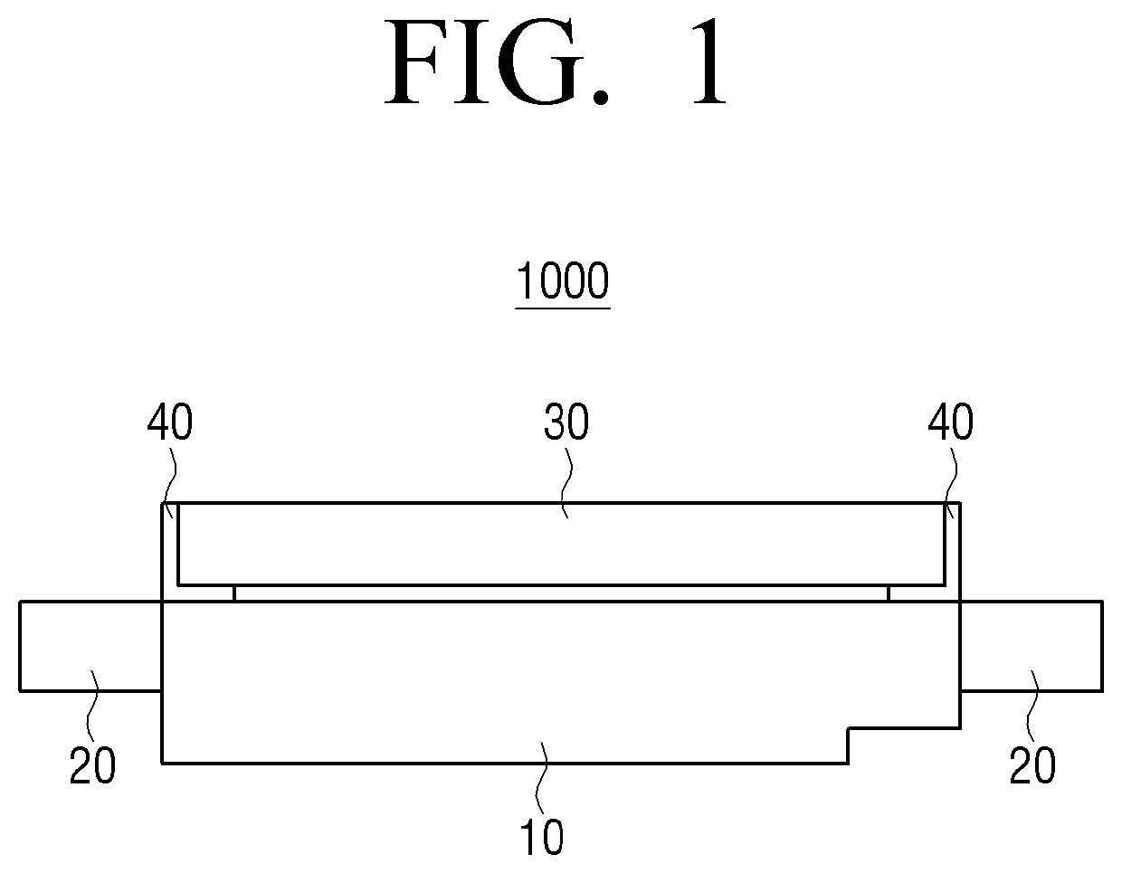
[0040]FIG. 1 is a block diagram illustrating a light emitting diode (LED) apparatus 1000 according to an exemplary embodiment. Referring to FIG. 1, an LED apparatus 1000 includes a light emitting diode 10, a light leakage preventing layer 20, a wavelength...


PUM

PropertyMeasurementUnit
sizeaaaaaaaaaa
wavelengthaaaaaaaaaa
wavelength convertingaaaaaaaaaa

Abstract

A manufacturing method of a light emitting diode apparatus is provided. This method includes forming a light emitting diode on the substrate, forming a light leakage preventing layer to surround the side surface of the light emitting diode, etching a region corresponding to the light emitting diode in the substrate, and bonding a wavelength converting material to a lower portion of the light emitting diode in the etched region, in which the wavelength converting material includes a semiconductor layer including a quantum well layer.

Description

CROSS-REFERENCE TO RELATED APPLICATIONS[0001]This application is based on and claims priority under 35 U.S.C. § 119 to Korean Patent Application No. 10-2017-0134562, filed on Oct. 17, 2017, in the Korean Intellectual Property Office, the disclosure of which is incorporated by reference herein in its entirety.BACKGROUND1. Field[0002]Apparatuses and methods consistent with what is disclosed herein broadly relate to an LED apparatus and a manufacturing method thereof, and more particularly, to an LED apparatus that can be manufactured in an extremely small size and manufacturing method thereof.2. Description of Related Art[0003]2-Dimensional LED elements, in related art, use III-V group semiconductor materials (Ga, In, Al) to control the optical energy bandgap through the material type, thickness, and doping process of the active layer, thereby inducing a single color such as red, green, and blue. The semiconductor layer included in the active layer may be deposited by Metal-Organic Ch...

Claims


Application Information

Patent Timeline
Patent Type & Authority Patents(United States)
IPC IPC(8): H01L33/50H01L25/075H01L33/60H01L33/20H01L33/46H01L33/00H01L33/62
CPCH01L33/60H01L33/46H01L33/502H01L25/0756H01L33/62H01L33/0093H01L33/20H01L2933/0066H01L2933/0041H01L2933/0058H01L33/005H01L33/501H01L33/06H01L33/44H01L33/10H01L33/58
Inventor KANG, JIN-HEEKANG, JI-HOONCHO, SEONG-WOO
Owner SAMSUNG ELECTRONICS CO LTD
Features
  • R&D
  • Intellectual Property
  • Life Sciences
  • Materials
  • Tech Scout
  • Unparalleled Data Quality
  • Higher Quality Content
  • 60% Fewer Hallucinations
Learn More