Process for making electronic device

a technology of electronic devices and processing methods, applied in semiconductor devices, solid-state devices, photovoltaic energy generation, etc., can solve the problems of reduced device performance, reduced device performance, and reduced device performance, so as to improve device performance, improve device performance, and reduce the effect of aging

Active Publication Date: 2021-01-12
MERCK PATENT GMBH
View PDF9 Cites 0 Cited by
  • Summary
  • Abstract
  • Description
  • Claims
  • Application Information

AI Technical Summary

Benefits of technology

[0023]The inventors have surprisingly found that the above-mentioned process for the preparation of an electronic device allows an efficient and controlled deposition of organic functional materials to form uniform functional layers having good layer properties and performance. In particular, the preparation process according to the present invention allows the formation of well-defined and uniform interfaces without defects between two adjacent functional layers. This is due to a kinetic control which prevents detachment, partial dissolution, redissolution or other impairment of the first functional layer on which the second functional layer is printed on top.
[0024]Moreover, it was found that the above-mentioned process for the preparation of an electronic device contains fewer process steps as compared to the prior art and is therefore easier, faster and more cost efficient. Beyond that, OLEDs which are produced by said preparation process show improved device performance such as improved lifetime. In addition there is no need for a cross-linking of the first organic functional material or other treatment to prevent solubility of the first functional layer on which the second organic functional material is deposited to form the second functional layer.

Problems solved by technology

One of the main challenges in multi-layer printing is to identify and adjust the respective printing parameters in order to obtain a homogeneous deposition of inks on the substrate thereby creating well-defined and uniform functional layers which give good device performance.
In multi-layer printing processes, there is always the risk of a detachment, partial dissolution, redissolution or other impairment of the existing functional layers on the substrate on which a new functional layer is printed.
This results in defects in the functional layers' interface which leads to a lower device performance.
The process is thus characterized by a high complexity and requires complex equipment for production.
However, the second solvent is selected such that the first organic compound is not soluble therein.
However, the concept of orthogonal solvents has the following drawbacks: Using orthogonal solvents to prepare successive solution-processed layers in electronic devices is usually achieved by choosing a solvent pair which has a strong difference in polarity (e.g. an non-polar organic solvent and an aqueous solvent) or chemical composition (e.g. a hydrocarbon solvent and a highly fluorinated solvent).
This reduces the degrees of freedom for material design and therefore restrains the optimization of the performance of a material in its function in the electronic device.
Another drawback of the use of orthogonal solvents is the residual solvent in the thin films: Polar solvent (like water) are known to be detrimental to device performance parameters like the lifetime of the device.
Residual solvent in the thin film, especially for the fluorinated solvents also affects the surface energy of thin films which leads to wettability problems during the solution-deposition on top of these layers.

Method used


Image

  • Process for making electronic device
  • Process for making electronic device
  • Process for making electronic device

Examples


working examples

Dissolution Tests

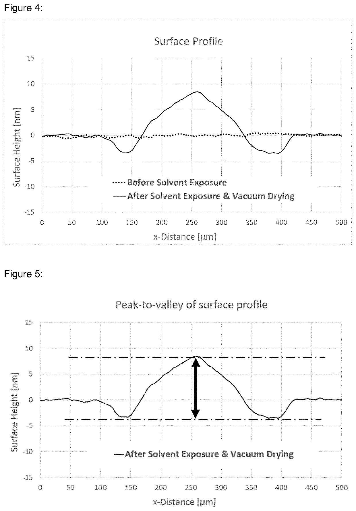
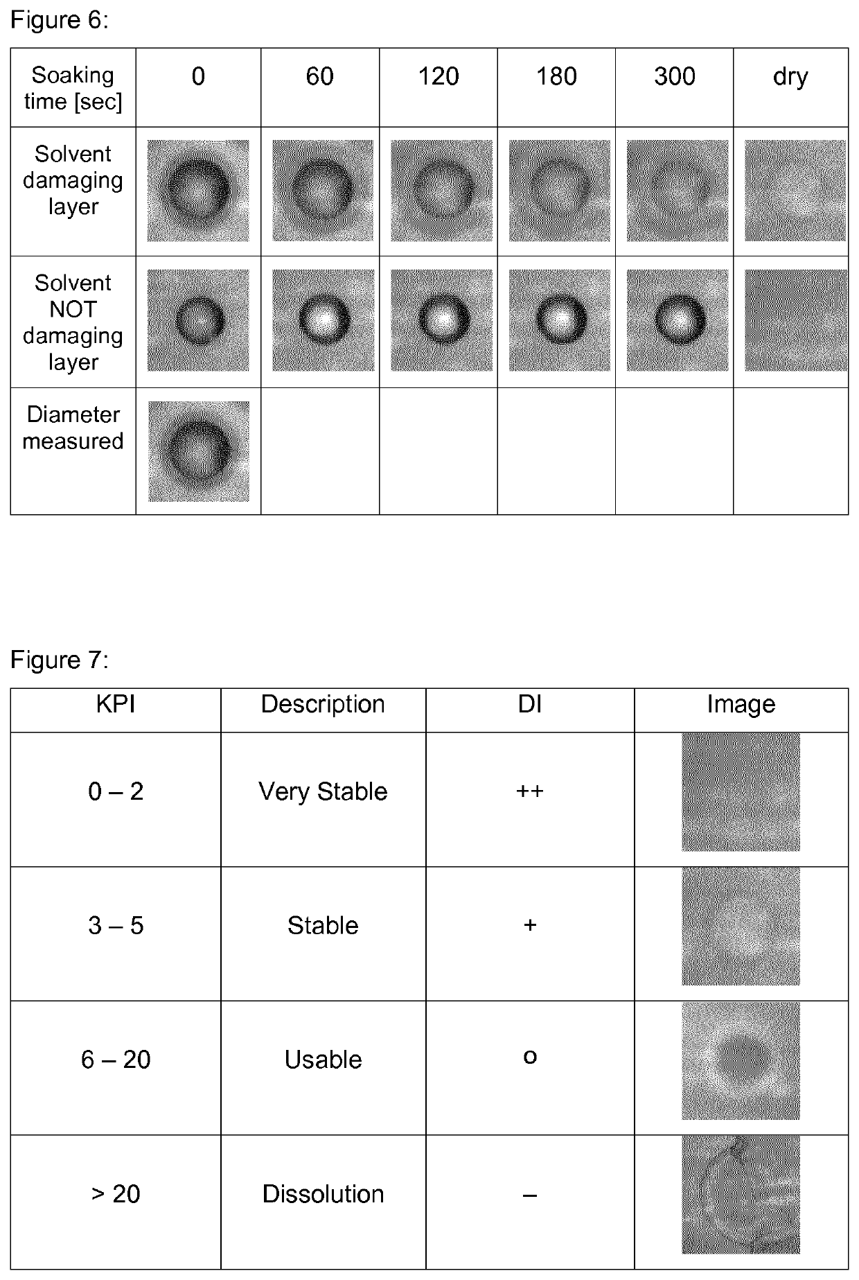
[0309]The determination of the solubility of a material in a solvent can be performed following ISO norm 7579:2009, which describes solubility determination by photometric or gravimetric methods. The photometric technique is recommended here, since the boiling points of the solvents considered are higher than 120° C.

[0310]Dissolution tests as described in the following were performed. The experiment was designed with particular focus on ease of reproducibility. The material(s) to be analyzed (which are used to form the first functional layer) were weighed into a transparent glass flask. A solvent (or a preformed solvent mixture) belonging to the list established in Table 3 was then added to the solid mixture at once, calculated to reach a final concentration of 7 g / L. The mixture was stirred at 600 rpm using a magnetic stirrer and at room temperature (25° C.) until complete dissolution, which was judged by visual inspection of the mixture. Towards the end of the dis...


PUM

PropertyMeasurementUnit
absolute solubilityaaaaaaaaaa

Abstract

Described herein is a process for the preparation of an electronic device such as an organic electroluminescent device (OLED), wherein two adjacent functional layers having an interface are formed from solution in a kinetically controlled manner. The process is particularly suitable for fast and efficient production of electronic devices by printing or coating processes. The description further relates to an electronic device which is obtainable by said process.

Description

CROSS-REFERENCE TO RELATED APPLICATIONS[0001]This application is a national stage application (under 35 U.S.C. § 371) of PCT / EP2017 / 081305, filed Dec. 4, 2017, which claims benefit of European Application No. 16202544.9, filed Dec. 6, 2016, both of which are incorporated herein by reference in their entirety.TECHNICAL FIELD[0002]The present invention relates to a process for the preparation of an electronic device such as an organic electroluminescent device (OLED), wherein two adjacent functional layers having an interface are formed from solution in a kinetically controlled manner. The process is particularly suitable for a fast and efficient production of electronic devices by printing or coating processes. The present invention furthermore relates to an electronic device which is obtainable by said process.BACKGROUND ART[0003]Traditionally, OLEDs have been fabricated by vacuum deposition for small molecule materials, and by spin-coating or dip coating for polymeric materials. Mo...

Claims


Application Information

Patent Timeline
Patent Type & Authority Patents(United States)
IPC IPC(8): H01L51/00H01L51/50
CPCH01L51/0007H01L51/5012H01L51/5056Y02E10/549H10K71/15H10K50/15H10K50/11
Inventor BÉALLE, GAELLELEONHARD, CHRISTOPHTSENG, HSIN-RONGHAMBURGER, MANUELBURKHART, BEATESCHEIBLE, KATJA MARIAJATSCH, ANJA
Owner MERCK PATENT GMBH
Why Eureka
Try Eureka