Supercharge Your Innovation With Domain-Expert AI Agents!

Encapsulation method for flip chip

a technology of encapsulation method and flip chip, which is applied in the manufacture of semiconductor/solid-state devices, electrical apparatus, and semiconductor devices. it can solve the problems of reducing the reliability and thermal conductivity of the encapsulation method of solder paste and elargol, unable to be used for encapsulation of high-power flip chips, and putting a greater stress on the chip

Active Publication Date: 2021-04-20
KE QUAN
View PDF25 Cites 0 Cited by
  • Summary
  • Abstract
  • Description
  • Claims
  • Application Information

AI Technical Summary

Benefits of technology

This method enhances positional accuracy, simplifies the process, improves production efficiency, and effectively reduces thermal resistance, making it suitable for high-power flip chips by ensuring reliable and efficient heat dissipation.

Problems solved by technology

But no matter what method is used, high precision die bonding is necessary because the distance between positive and negative electrodes of the flip chip can't be very large; flip chip eutectic technology involves expensive production equipment and materials, which makes it costly and advantage of cost performance can't be reflected, and encapsulation method of solder paste and elargol are limited to lower reliability and poorer thermal conductivity, and can't be used for encapsulation of a high-power flip chip, and flip-LED technology has been come out for a long time, but limited by many reasons, it delays popularizing.
CN104658929A), is that after the chip and the metal substrate being bonded, the metal substrate is cut along an insulating region between electrodes on the chip by means of laser cutting or the like to cut off electrical connection between electrodes of the chip, thus cutting off electrical connection between electrodes of the corresponding chip, but a hidden danger of this method is that this cutting action will lead to greater stress on the chip, although it is only cutting metal, it might pass through two electrodes that have been fixed, thus adversely affecting the chip.

Method used


Image

  • Encapsulation method for flip chip
  • Encapsulation method for flip chip
  • Encapsulation method for flip chip

Examples


embodiment 1

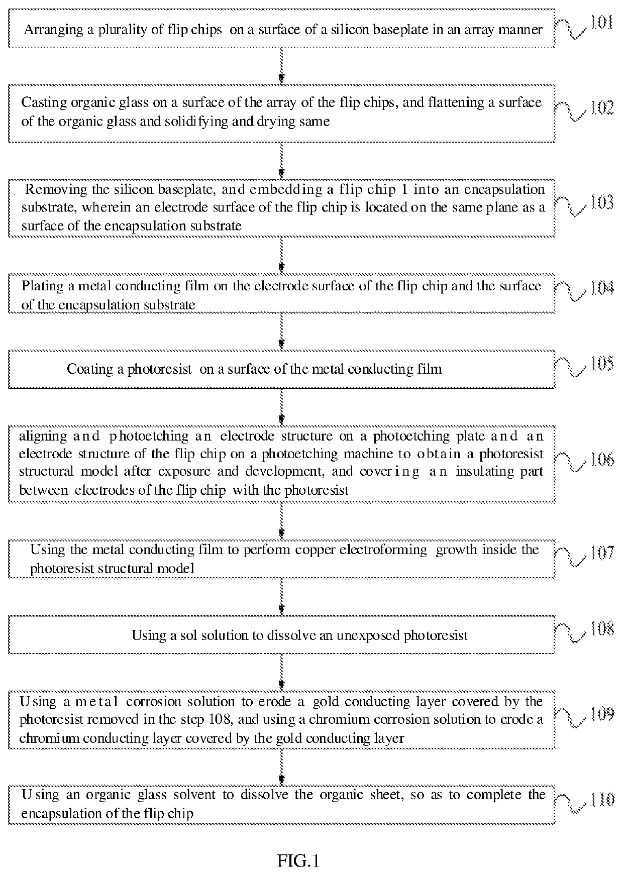
[0062]As shown in FIG. 1, the encapsulation method for the flip chip in the embodiment comprises the following steps:

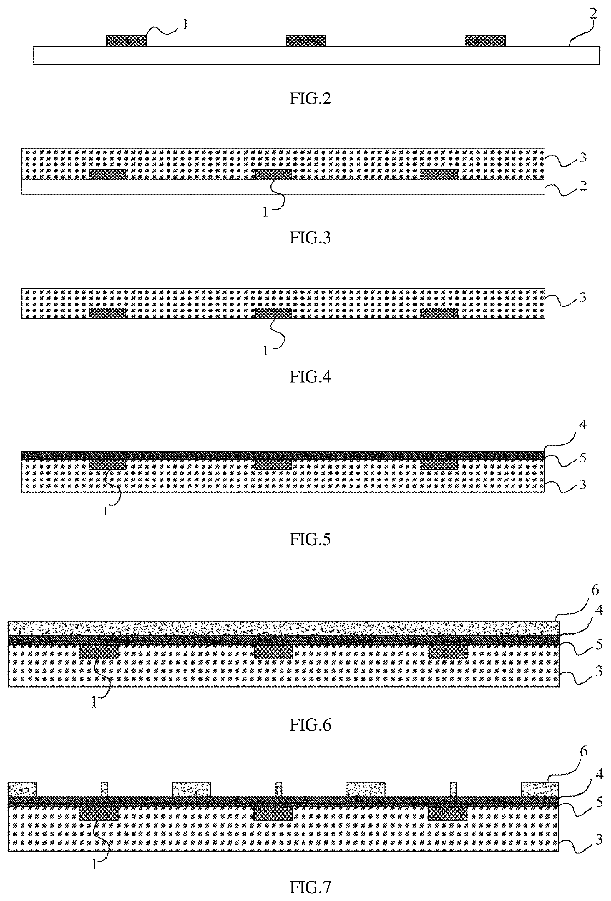
[0063]Step 101, arranging a plurality of flip chips 1 on a surface of a silicon baseplate 2 in an array manner, and contacting the electrode surface of the flip chip 1 with a surface of the silicon baseplate 2, wherein, preferably, the distance between two adjacent flip chips 1 is 6 mm, and a schematic structural diagram of an intermediate product obtained after performing the step 101 is as shown in FIG. 2.

[0064]Step 102, casting organic glass 3 on a surface of the array of the flip chips 1, and flattening a surface of the organic glass 3 and solidifying and drying the organic glass 3 to form an organic sheet having a thickness of 2 mm, and the organic sheet is used as an encapsulation substrate, and a schematic structural diagram of an intermediate product obtained after performing the step 102 is as shown in FIG. 3.

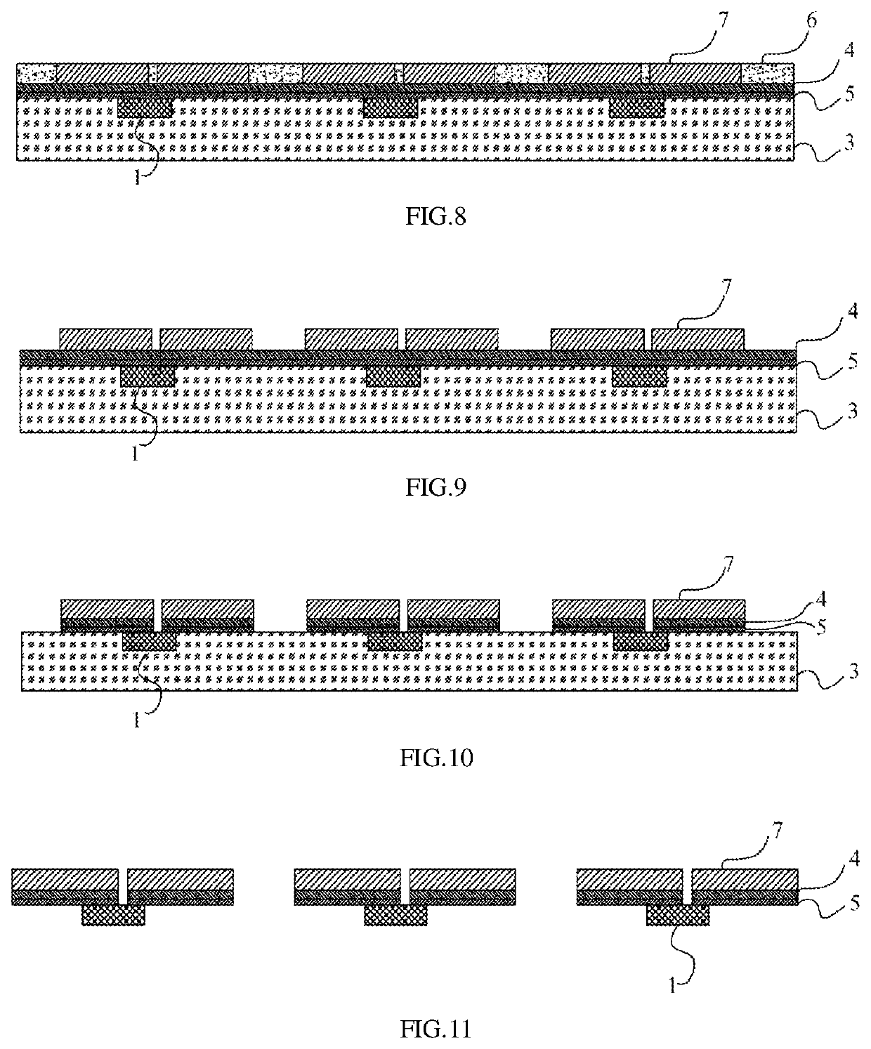
[0065]Step 103, removing the silicon baseplate 2, ...

embodiment 2

[0074]The main difference between this embodiment and the embodiment 1 lies in that: in this embodiment, the encapsulation substrate is a ceramic encapsulation substrate. As shown in FIG. 12, the encapsulation method for the flip chip in the embodiment comprises the following steps:

[0075]Step 201, a plurality of flip chips 1 are embedded in the ceramic encapsulation substrate 8, and in the embodiment, the flip chips are specifically LED flip chips of 1 mm in length, 1 mm in width and 0.35 mm in thickness, and the type is specifically CREEDA1000, and specific operations are as follows: providing a ceramic encapsulation substrate 8 having a thickness (about 0.6 mm) slightly larger than the thickness of the flip chip 1, and the unit center of each ceramic encapsulation substrate 8 is provided with a hollow notch which is consistent with the shape of the chip but slightly larger in size, and the substrate 8 having a side surface provided with a metal layer corresponding to and insulated...


PUM

PropertyMeasurementUnit
distanceaaaaaaaaaa
thicknessaaaaaaaaaa
thicknessaaaaaaaaaa

Abstract

An encapsulation method for a flip chip that includes electroforming metal on an electrode surface of a flip chip and a surface of an encapsulation substrate simultaneously. The encapsulation method specifically includes setting an encapsulation substrate around a flip chip; plating a metal conducting film on an electrode surface of the flip chip and a surface of the encapsulation substrate; coating a photoresist on a surface of the metal conducting film; aligning and photoetching an electrode structure on a photoetching plate and an electrode structure of the flip chip, and covering an insulating part between electrodes with the photoresist; taking the metal conducting film as the electrode, electroforming metal inside the photoresist structural model; and removing the photoresist covering the insulating part and removing the metal conducting film. The encapsulation method adopts electroforming and photoetching technology, and thus the process is simplified and the production efficiency is improved.

Description

[0001]This application claims priority of a Chinese patent application CN201510579955.1 filed on Sep. 11, 2015. This application cites the full text of the above Chinese patent application.FIELD OF INVENTION[0002]The present invention relates to an encapsulation method for a flip chip, and more particularly, to an encapsulation method for a flip chip based on electroforming technology.PRIOR ARTS[0003]With the development of flip chip technology, especially the popularity of semiconductor LED (light emitting diode) lighting, the use of flip encapsulation for semiconductor LED chips has become a trend, and the flip encapsulation generally uses three kinds of methods i.e. eutectic, solder paste and elargol for die bonding. But no matter what method is used, high precision die bonding is necessary because the distance between positive and negative electrodes of the flip chip can't be very large; flip chip eutectic technology involves expensive production equipment and materials, which m...

Claims


Application Information

Patent Timeline
Patent Type & Authority Patents(United States)
IPC IPC(8): H01L33/62H01L21/56H01L21/283H01L33/00H01L33/52
CPCH01L33/62H01L21/283H01L21/568H01L33/005H01L33/52H01L2224/04105H01L2224/19H01L2224/96H01L2924/18162H01L2933/0066H01L24/80H01L24/96H01L33/48
Inventor KE, QUANYI, FUTINGPAN, MING
Owner KE QUAN
Features
  • R&D
  • Intellectual Property
  • Life Sciences
  • Materials
  • Tech Scout
  • Unparalleled Data Quality
  • Higher Quality Content
  • 60% Fewer Hallucinations
Learn More