Mask and method of manufacturing the same

a manufacturing method and mask technology, applied in the field of masks and a manufacturing method, can solve the problems of difficult to obtain high-resolution patterns, difficult to precisely control pattern width, and high attention, and achieve the effects of minimizing damage to masks, easy peeling off masks, and high surface roughness

Active Publication Date: 2021-08-10
LG DISPLAY CO LTD
View PDF3 Cites 0 Cited by
  • Summary
  • Abstract
  • Description
  • Claims
  • Application Information

AI Technical Summary

Benefits of technology

[0008]An object to be achieved by the present disclosure is to provide a mask and a method of manufacturing the mask. In the mask, a partial region of a plating layer has a high surface roughness to easily peel off the mask from a substrate and thus minimize damage to the mask during a process.
[0009]Another object to be achieved by the present disclosure is to provide a mask and a method of manufacturing the mask. An align key region formed on a surface of the mask has a reduced reflectance, and, thus, a detection rate for an align key can be improved and the mask can be easily disposed at a desired position.
[0010]Yet another object to be achieved by the present disclosure is to provide a method of manufacturing a mask using two or more conductive layers with different resistances. In the mask, a plating layer to be formed by electroplating can be easily peeled off and has high uniformity in thickness.
[0017]According to the present disclosure, a mask includes a partial region with a higher surface roughness than its peripheral region. Thus, it is possible to easily peel off the mask from a substrate and minimize damage to the mask during the manufacturing process.
[0018]According to the present disclosure, an align key with a high surface roughness is formed. Thus, by reducing the reflection using the high surface roughness, it is possible to increase a detection rate of the align key and easily align the mask.
[0019]According to the present disclosure, a first conductive layer and a second conductive layer having different properties are used as seed layers. Thus, it is possible to easily peel off the mask during the manufacturing process and form a mask with a uniform thickness.

Problems solved by technology

Therefore, the OLED has been attracting a lot of attention.
However, when the mask is manufactured using the wet-etching process, it is difficult to precisely control the pattern width during the etching process due to the isotropy of etching.
Therefore, it is difficult to obtain a high-resolution pattern.

Method used


Image

  • Mask and method of manufacturing the same
  • Mask and method of manufacturing the same
  • Mask and method of manufacturing the same

Examples


experimental example

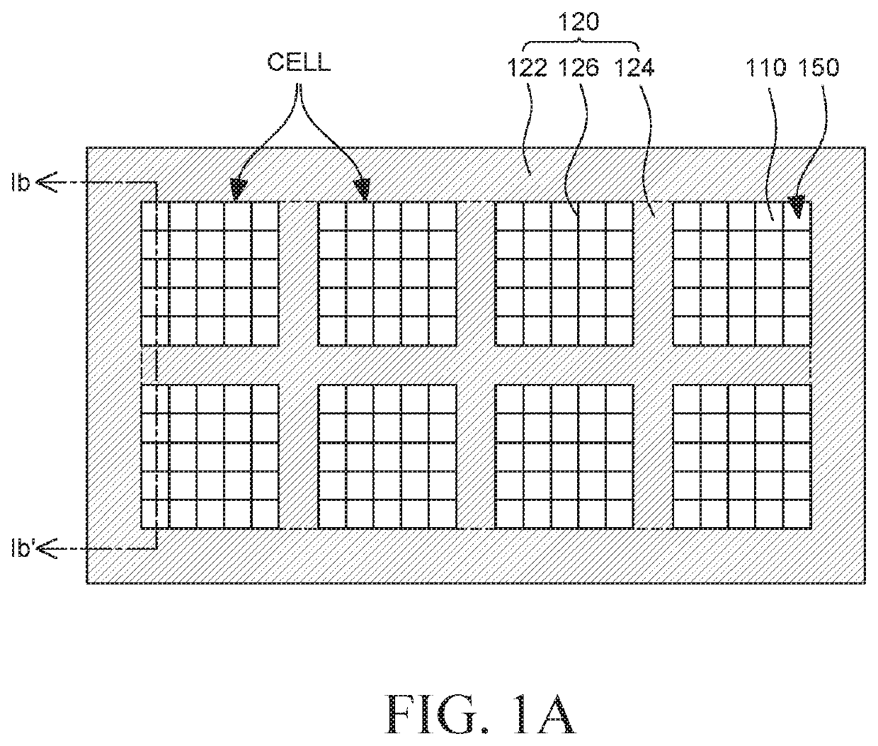
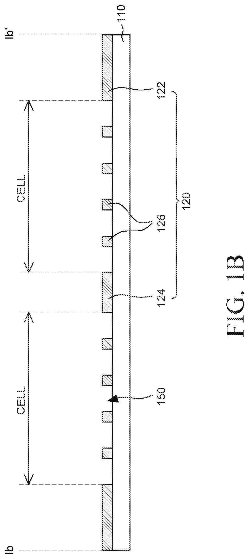
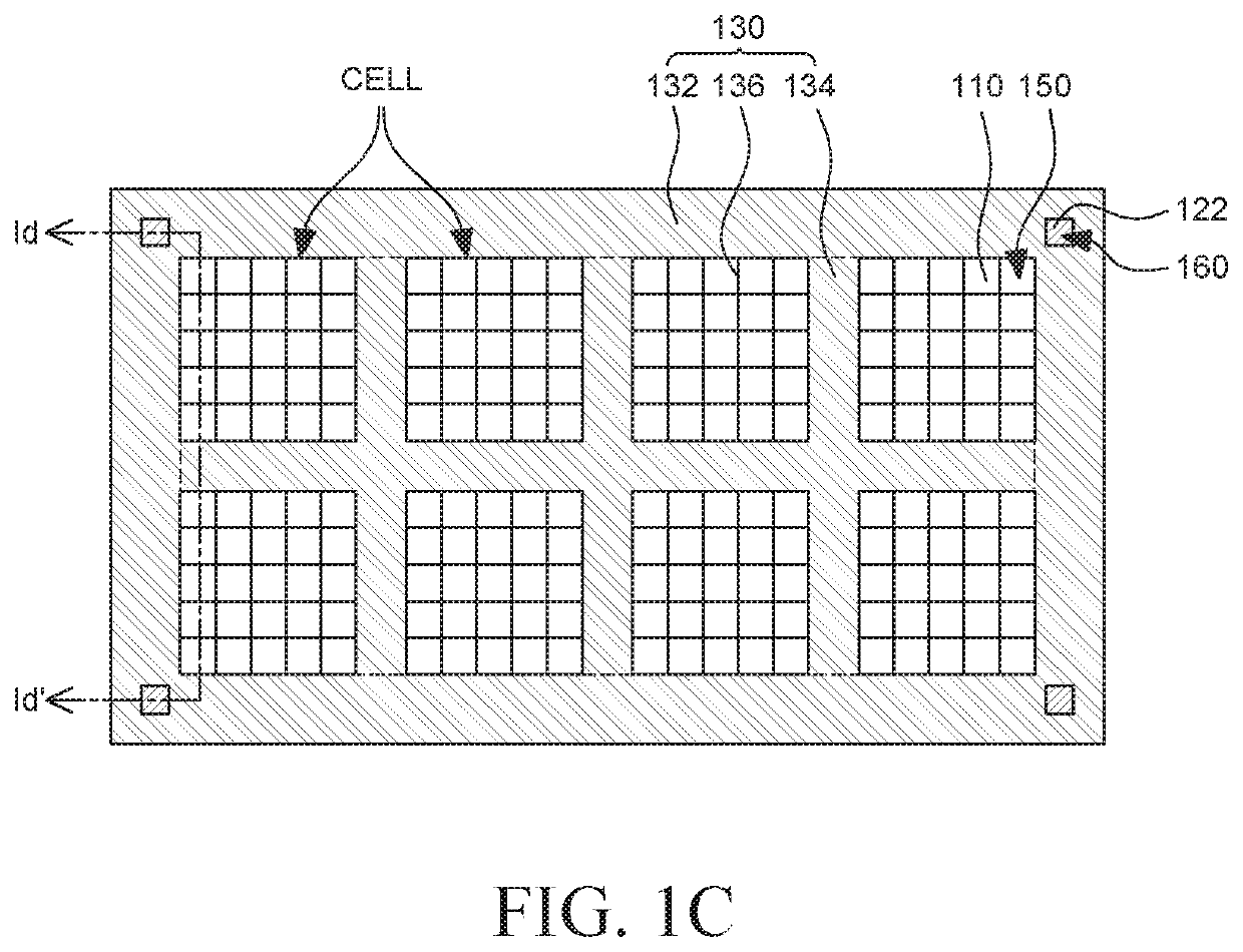
[0121]A first conductive layer was sputtered on a substrate, and a second conductive layer was sputtered on the first conductive layer and electroplating was performed to form a mask. Then, a plating layer was separated from the substrate, the first conductive layer, and the second conductive layer to manufacture a mask.

[0122]In Example 1, molybdenum (Mo) was used for the first conductive layer and polycrystalline-indium tin oxide (poly-ITO) was used for the second conductive layer. In Example 2, a double layer of molybdenum-titanium alloy (MoTi) and copper (Cu) was used for the first conductive layer and poly-ITO was used for the second conductive layer.

[0123]In Comparative Example 1, poly-ITO was used for a single conductive layer and in Comparative Example 2, molybdenum (Mo) was used for a single conductive layer, and then electroplating was performed thereto. In Comparative Example 3, a double conductive layer formed of molybdenum-titanium alloy (MoTi) and copper (Cu) was used a...


PUM

PropertyMeasurementUnit
surface roughnessaaaaaaaaaa
conductiveaaaaaaaaaa

Abstract

Provided is a method of manufacturing a mask includes preparing a first conductive layer. The first conductive layer includes a third portion having a mesh shape in a plurality of cell regions on a substrate, a second portion disposed between the cell regions, and a first portion surrounding the third portion and the second portion. The method further includes preparing a second conductive layer including at least one opening on the first conductive layer. The method also includes oxidizing a part of the first conductive layer exposed through the at least one opening of the second conductive layer. The method further includes preparing a plating layer on the first conductive layer and the second conductive layer, and removing the first conductive layer and the second conductive layer from the plating layer.

Description

CROSS-REFERENCE TO RELATED APPLICATIONS[0001]This application claims the priority of Korean Patent Application No. 10-2018-0171804 filed on Dec. 28, 2018, in the Korean Intellectual Property Office, the disclosure of which is incorporated herein by reference.BACKGROUNDTechnical Field[0002]The present disclosure relates to a mask and a method of manufacturing the same, and more particularly, to a mask for use in a manufacturing process of an organic light emitting display device to deposit an organic layer and formed by a plating process and a method of manufacturing the same.Description of the Related Art[0003]As the information age advances, the field of a display device for visually displaying electrical information signals has grown rapidly. In accordance with the rapid development, various display devices having excellent performance such as thin thickness, light weight, and low power consumption properties have been developed. Specific examples of the above-mentioned display de...

Claims


Application Information

Patent Timeline
Patent Type & Authority Patents(United States)
IPC IPC(8): C23C14/04C23C14/14C23C14/08C23C14/58C23C14/34C23C8/10H01L51/00
CPCC23C14/042C23C8/10C23C14/086C23C14/14C23C14/34C23C14/5846C23C14/5873H01L51/0011C23C14/12H10K71/164H10K71/166C23C14/165H10K71/00G03F7/2063H10K71/233C23C14/24
Inventor KIM, HYUNJUN
Owner LG DISPLAY CO LTD
Why Eureka
Try Eureka