

Functional contactor
a contactor and functional technology, applied in the field of contactors, can solve the problems of inability to reduce manufacturing costs, inconvenient mass production, and injury to users, and achieve the effects of reducing manufacturing costs and processing time, reducing galvanic corrosion, and easy manufacturing
- Summary
- Abstract
- Description
- Claims
- Application Information
AI Technical Summary
Benefits of technology
Problems solved by technology
Method used
Image


Examples
first embodiment
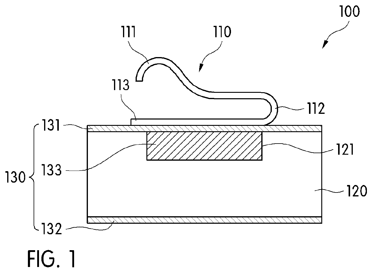
[0040]As shown in FIGS. 1 and 2, a functional contactor 100 according to the present invention includes a conductive elastic portion 110, a substrate 120, and a functional element 130.
[0041]In a portable electronic device, the functional contactor 100 is configured to electrically connect a conductive case such as an external metal case to a circuit substrate or to electrically connect the conductive case to a conductive bracket electrically coupled to one side of the circuit substrate.
[0042]That is, in the functional contactor 100, the conductive elastic portion 110 may come into contact with the circuit substrate or the conductive bracket and the substrate 120 may be coupled to the conductive case. Contrarily, the conductive elastic portion 110 may come into contact with the conductive case and the substrate 120 may be coupled to the circuit substrate.
[0043]For example, when the functional contactor 100 is a functional contactor of a surface mount technology (SMT) type, i.e., the ...
second embodiment
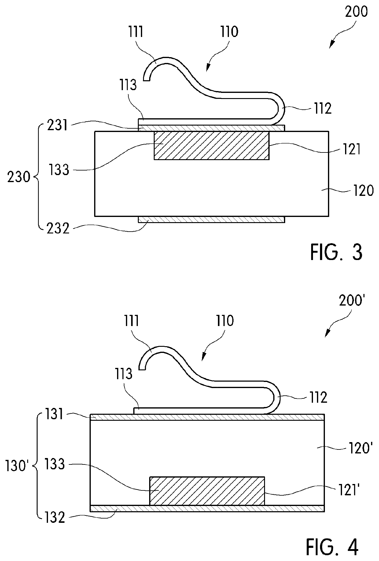
[0098]As shown in FIGS. 9 and 10, a functional contactor 300 according to the present invention includes a conductive elastic portion 310, a substrate 320, and a functional element 330.
[0099]A configuration of the conductive elastic portion 310 is identical to that of the conductive elastic portion 110 of the first embodiment, and thus a detailed description thereof will be omitted.
[0100]The substrate 320 is comprised of a plurality of dielectric layers 321, 322, and 323. For example, the substrate 320 may be comprised of three dielectric layers 321, 322, and 323. That is, the three dielectric layers 321, 322, and 323 are disposed between a first electrode 331 and a second electrode 332 and are sequentially stacked on the second electrode 332. The first dielectric layer 321 may be disposed at a lowermost portion of the substrate 320, the second dielectric layer 322 may be disposed on the first dielectric layer 321, and the third dielectric layer 323 may be disposed on the second die...
PUM
 Abstract
Description
Claims
Application Information