Scanning probe microscopy system for and method of mapping nanostructures on the surface of a sample

a microscopy system and nanostructure technology, applied in the field of scanning probe microscopy system for mapping nanostructures on the surface of samples, can solve the problems of high resolution and accuracy of microscopic probes, high processing costs, unrealistic or at least cumbersome, etc., and achieve the effect of increasing throughput, accuracy and footprin

Active Publication Date: 2022-05-03
NEDERLANDSE ORG VOOR TOEGEPAST-NATUURWETENSCHAPPELIJK ONDERZOEK (TNO)
View PDF10 Cites 0 Cited by
  • Summary
  • Abstract
  • Description
  • Claims
  • Application Information

AI Technical Summary

Benefits of technology

[0006]It is an object of the present invention to overcome the disadvantages described above, and to provide a scanning probe microscopy system and method providing increased performance in terms of throughput, accuracy and footprint.
[0010]The present invention applies a common path type optical sensor device that provides a common path reference signal and sensed signal, and wherein a sensed fraction is transmitted to the probe tip whereas a reflected fraction thereof is received by the same directional optics to provide the sensed signal. The invention is thereby based on the insight that by doing so, an interferometer may be applied to directly measure the absolute distance between the directional optics of the sensor and the exact position of the probe tip. From the output signal of the interferometer, both the static behavior and the dynamic behavior is therefore derivable. This may be achieved, for example, by analyzing the output signal in a certain frequency range associated with either one of the static and dynamic behavior. For example, all signal components below 2 kilohertz (kHz) may be associated with static behavior, whereas all signal components above 2 kHz may relate to dynamic behavior. A threshold frequency may thus be applied to identify the signal component as being associated with static or dynamic behavior, the threshold for example being within a range of 1 kilohertz to 10 kilohertz, preferably within a range of 1 kilohertz to 5 kilohertz, more preferably at or around 2 kilohertz. In accordance with some embodiments, either one of low pass filters, high pass filters or band pass filters may be applied to separate out a particular frequency range for further analysis of either the static or dynamic behavior. Such filter may apply first and second filter frequencies, e.g. set at the abovementioned threshold or at particular frequency values relating to particular signal components. Moreover, in some embodiments, digital processing allows to analyze the output signal in certain frequency ranges. Such signal processing may apply fast Fourier transforming (FFT) or a different digital processing technique to analyze certain frequency components. Moreover, combinations of analogue and digital processing may be applied. In principle, one of the advantages of the system of the present invention is that it enables the application of analogue signal processing techniques, which are fast and robust.
[0014]The abovementioned embodiments applying multiple mixed signals of different path lengths, enable to very accurately determine the distance variation across a large range of distances. The common path architecture eliminates effects of differences in temperature or mechanical variation of the paths. Nevertheless, variation of the common path may still affect sensing results in a conventional interferometer. Basically, the interference intensity as a function of distance to the target is the sum of a constant term and a periodic term, the phase position in this period depending on a ratio between the distance and the wavelength. By counting the number of periods, wavelength accuracy is possible. The distance could be determined with sub-wavelength accuracy from the intensity obtained from the common path architecture and hence the phase measurement, when the amplitudes of the constant term and the periodic term would be known. However, variation of the common path affects these amplitudes, and hence the determination of the distance. In the common path architectures described in the above embodiments, sub-wavelength accurate path length difference measurement is possible due to the fact that different paths are coupled to different inputs of a three way coupler. This can be done across a large range of distances, hence enabling a highly accurate and direct measurement of the distance to the probe tip.

Problems solved by technology

The very high resolution and accuracy of a microscopic probe however comes at the cost of performance in terms of throughput.
For object of macroscopic dimensions this results in significant processing time, which may be unrealistic or at least cumbersome for practical use and altogether incompatible with on line use in manufacturing processes.

Method used


Image

  • Scanning probe microscopy system for and method of mapping nanostructures on the surface of a sample
  • Scanning probe microscopy system for and method of mapping nanostructures on the surface of a sample
  • Scanning probe microscopy system for and method of mapping nanostructures on the surface of a sample

Examples


Embodiment Construction

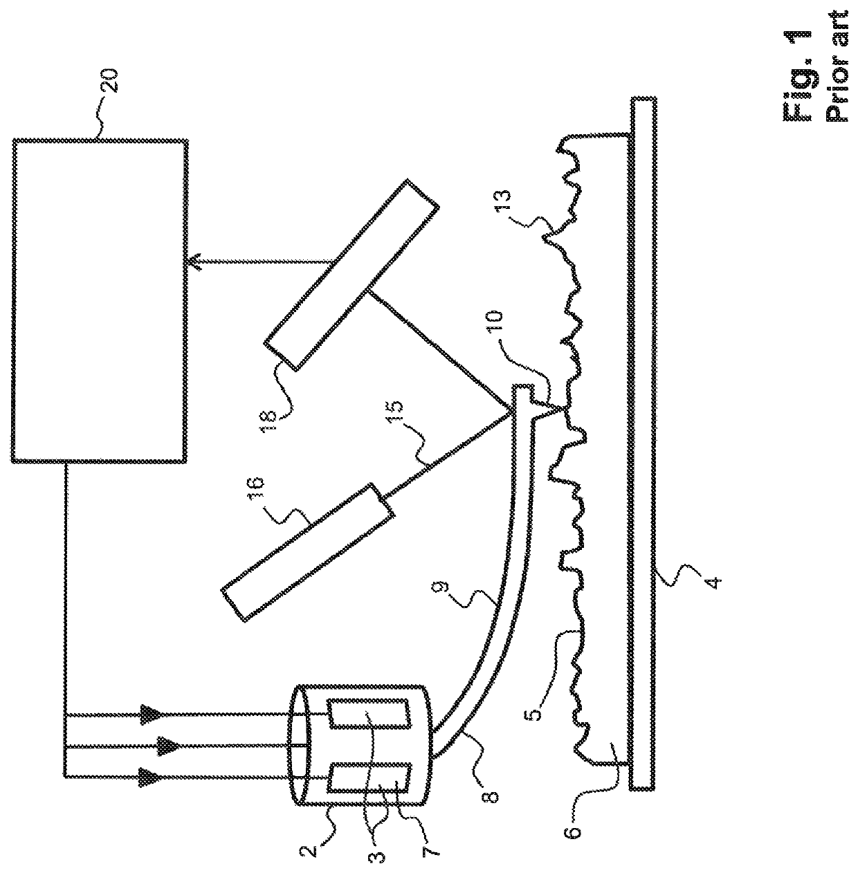
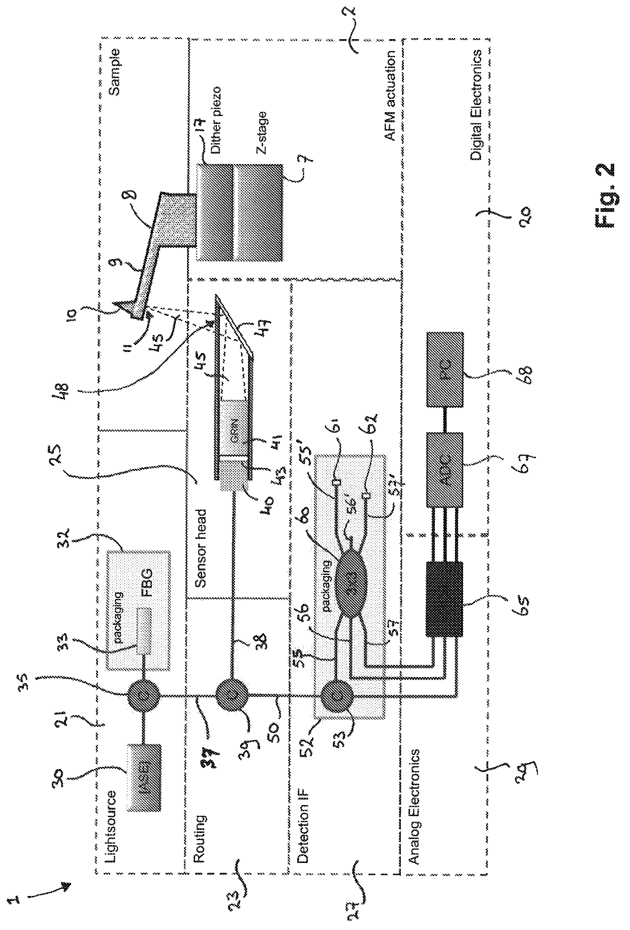
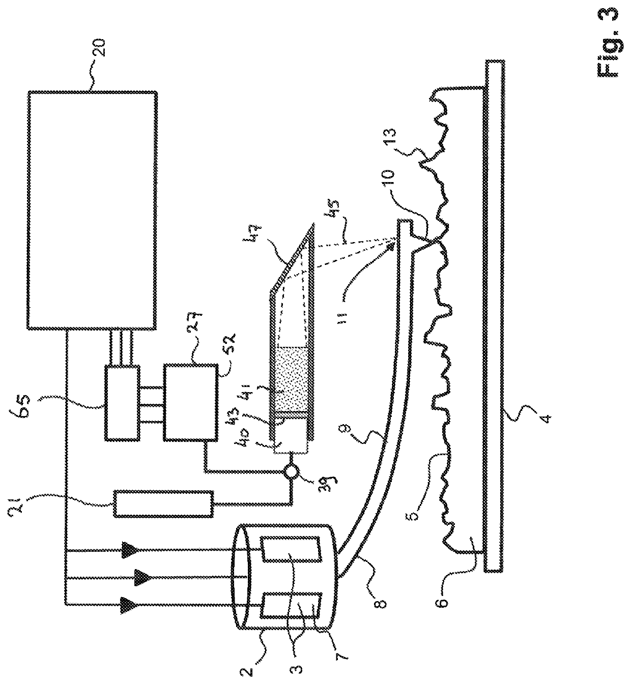
[0024]FIG. 1 schematically illustrates the working principle of a typical prior art atomic force microscope. In FIG. 1, a probe head 2 comprises piezo type drivers 3 for the X-, Y-, and Z-directional motion of a probe 8. The probe 8 consists of a cantilever 9 having a probe tip 10 arranged for scanning a sample surface 5 of a sample 6. During scanning, a dither piezo 17 (not shown in FIG. 1) or other means of actuations such as photo-thermal actuation, electrostatic, etc., may drive the cantilever in vibrational mode (for example close to resonant frequency) to enable tapping of the probe tip on the surface. The manner of applying a vibrational motion to the probe tip is known to the skilled person.

[0025]Scanning of the sample surface 5 is performed by moving the probe tip 10 in the X- and Y direction parallel to the sample surface 5 (or alternatively, by moving the substrate surface in the X- and Y-directions while maintaining the position of the probe tip fixed in the X- and Y-dir...


PUM

PropertyMeasurementUnit
frequencyaaaaaaaaaa
frequencyaaaaaaaaaa
frequencyaaaaaaaaaa

Abstract

The present document relates to a scanning probe microscopy system and method for mapping nanostructures on the surface of a sample. The system comprises a sample support structure, a scan head including a probe comprising a cantilever and a probe tip, and an actuator for scanning the probe tip relative to the sample surface. The system also includes an optical source, and a sensor unit for obtaining a sensor signal indicative of a position of the probe tip. The sensor unit includes a partially reflecting element for reflecting a reference fraction and for transmitting a sensing fraction of the optical signal. It further includes directional optics for directing the sensing fraction as an optical beam towards the probe tip, and for receiving a reflected fraction thereof to provide a sensed signal. Moreover the sensor includes an interferometer for providing one or more output signals, and signal conveyance optics for conveying the sensed signal and the reference signal to the interferometer. The directional optics is configured for directing the sensing fraction such that at least a part of the sensing fraction is reflected by the probe tip such as to form the reflected fraction.

Description

CROSS-REFERENCE TO RELATED APPLICATIONS[0001]This patent application is a U.S. National Phase of PCT International Application No. PCT / NL2018 / 050316, filed May 14, 2018, which claims priority to European Application No. 17171030.4, filed May 15, 2017, which are both expressly incorporated by reference in their entireties, including any references contained therein.FIELD OF THE INVENTION[0002]The present invention is directed at a scanning probe microscopy system for mapping nanostructures on the surface of a sample, comprising a sample support structure for supporting the sample, a scan head including a probe comprising a cantilever and a probe tip arranged on the cantilever, and an actuator for scanning the probe tip relative to the sample surface for mapping of the nanostructures, further comprising an optical source for providing an optical signal, and a sensor unit for obtaining a sensor signal indicative of a position of the probe tip during scanning. The invention is further d...

Claims


Application Information

Patent Timeline
Patent Type & Authority Patents(United States)
IPC IPC(8): G01Q20/02G01Q10/06G01Q60/24
CPCG01Q20/02G01Q10/065G01Q60/24G01B9/02028G01B9/02057G01B9/02065G01B9/02023G01B2290/45
Inventor SADEGHIAN MARNANI, HAMEDKASTELIJN, AUKJE ARIANNE ANNETTETOET, PETER MARTIJNKRAMER, GEERTEN FRANS IJSBRANDNIEUWKOOP, EVERTDEKKER, ALBERTVAN RIEL, MARTINUS CORNELIUS JOHANNES MARIAKRUIDHOF, RIK
Owner NEDERLANDSE ORG VOOR TOEGEPAST-NATUURWETENSCHAPPELIJK ONDERZOEK (TNO)
Why Eureka
Try Eureka