
High voltage device

a high-voltage device and high-voltage technology, applied in the direction of basic electric elements, electrical apparatus, inductance, etc., can solve the problems of insufficient isolation strength, difficult or even impossible to achieve such isolation level, dielectric layer isolation, etc., to improve the high-voltage capability of the device, reduce the electric field, and reduce the effect of electric field

Active Publication Date: 2022-06-07
X FAB DRESDEN
View PDF9 Cites 0 Cited by
  • Summary
  • Abstract
  • Description
  • Claims
  • Application Information

AI Technical Summary

Benefits of technology

This design significantly enhances isolation strength and reliability, allowing the device to withstand higher voltages while maintaining the same dielectric thickness, and can be integrated into standard CMOS processes at lower costs.

Problems solved by technology

It may be difficult or even not possible to achieve such level of isolation with the limitation of the isolation (dielectric) layers capability of available wafer fab processes.
This is because the stacking of the Inter Metal Dielectric layers in a CMOS process limits the isolation thickness to a few microns only, which is not sufficient to achieve a high enough isolation strength.

Method used


Image

  • High voltage device
  • High voltage device
  • High voltage device

Examples


Embodiment Construction

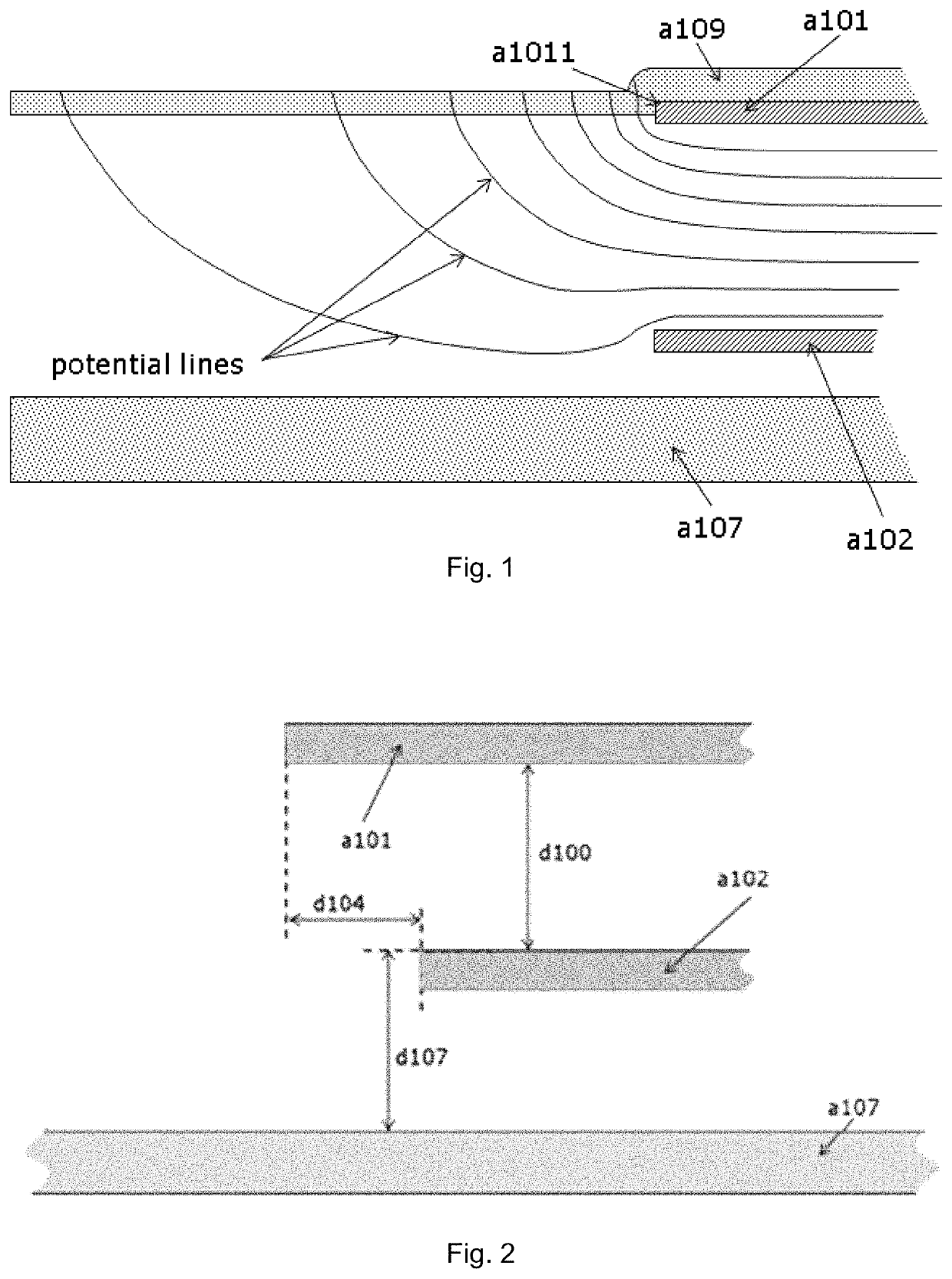
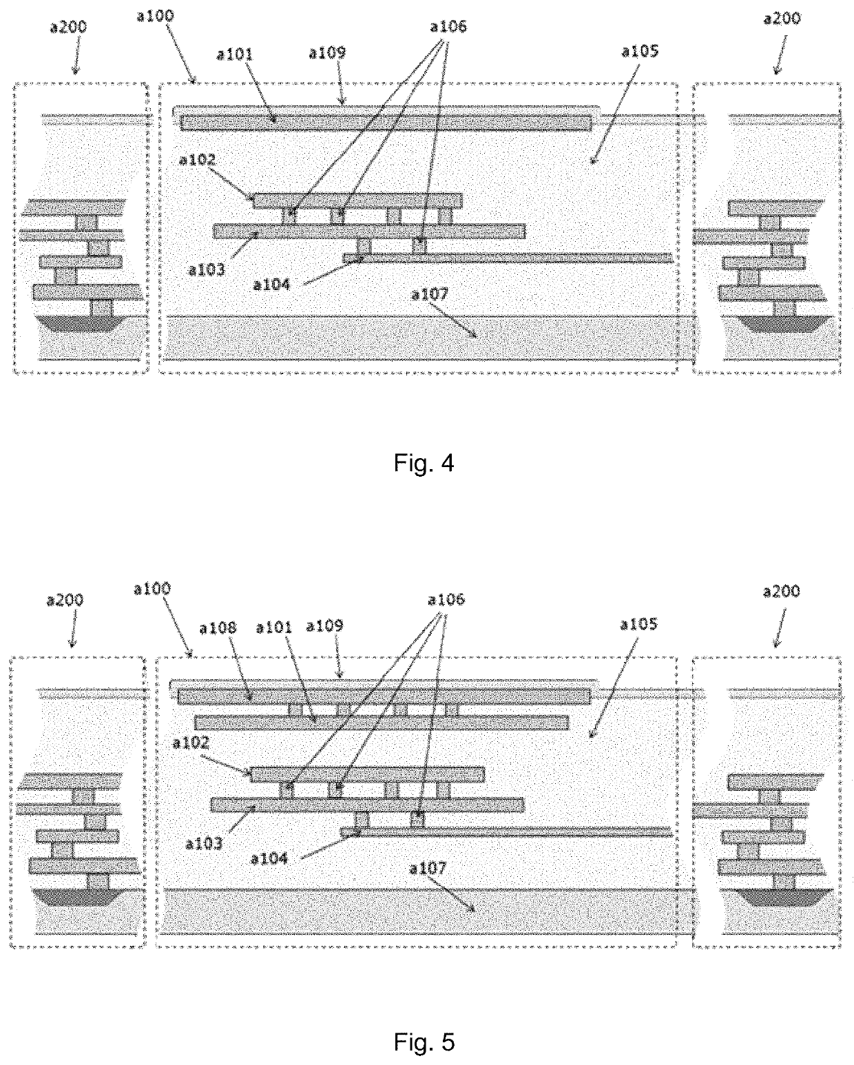
[0031]Some preferred embodiments of the disclosure will now be described by way of example only and with reference to the accompanying drawings, in which:

[0032]FIG. 1 illustrates a simulation of equipotential lines of the electric field a conventional HV component;

[0033]FIG. 2 shows a schematic illustration of a HV component, according to one embodiment of the disclosure;

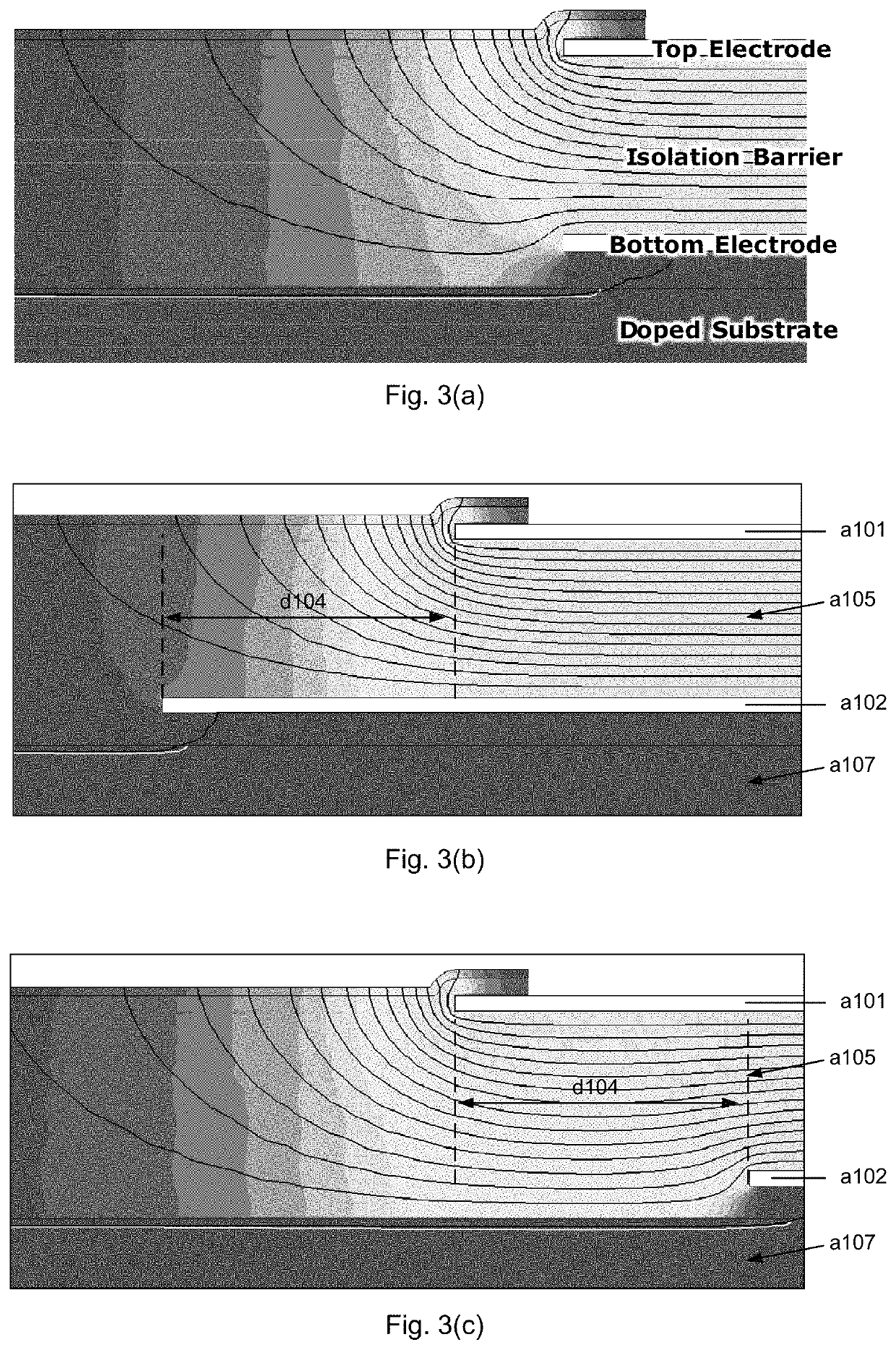
[0034]FIGS. 3(a)-3(c) illustrate simulations of the distribution of electrostatic potential for different overlap values between a first (top) electrode and a second (bottom) electrode within HV components;

[0035]FIG. 3(a) illustrates a simulation of electrostatic potential distribution within a component with symmetrical first and second electrodes;

[0036]FIG. 3(b) illustrates a simulation of electrostatic potential distribution within a component where the second (bottom) electrode extends beyond the first (top) electrode;

[0037]FIG. 3(c) illustrates a simulation of electrostatic potential distribution within a compo...


PUM

PropertyMeasurementUnit
thickness d100aaaaaaaaaa
thicknessaaaaaaaaaa
thicknessaaaaaaaaaa

Abstract

We disclose herein a high voltage device comprising: a first electrode; a second electrode disposed underneath and spaced from the first electrode; and a dielectric layer disposed between the first and second electrodes, wherein the first electrode extends further in at least one lateral direction in respect of the second electrode.

Description

[0001]This application claims priority to GB Application No. 1900931.5 filed Jan. 23, 2019, the entire contents of which are hereby incorporated by reference.TECHNICAL FIELD[0002]The present disclosure relates to a high voltage (H V) component or device for a microelectronic device, particularly but not exclusively, to a galvanic isolation device.BACKGROUND OF THE DISCLOSURE[0003]For several applications a high isolation capability between metal plates may be a key requirement. For galvanic isolation applications the requirements for the strength of isolation can be above 5 kV RMS (root mean square). It may be difficult or even not possible to achieve such level of isolation with the limitation of the isolation (dielectric) layers capability of available wafer fab processes. This is because the stacking of the Inter Metal Dielectric layers in a CMOS process limits the isolation thickness to a few microns only, which is not sufficient to achieve a high enough isolation strength. Ther...

Claims


Application Information

Patent Timeline
Patent Type & Authority Patents(United States)
IPC IPC(8): H01L21/00H01L49/02H01L21/02H01L21/8234H01L29/40H01L27/06H01L27/092H01L21/8238H10N97/00
CPCH01L28/60H01L21/02112H01L21/823481H01L21/823878H01L27/0629H01L27/0922H01L29/402H01L23/5223H01L27/0617H01L28/10
Inventor SIZOV, VICTORRESO, DENIS
Owner X FAB DRESDEN
Learn More