

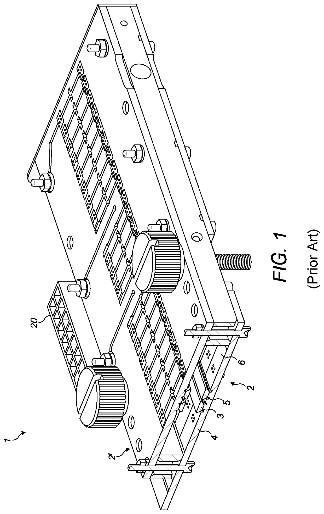
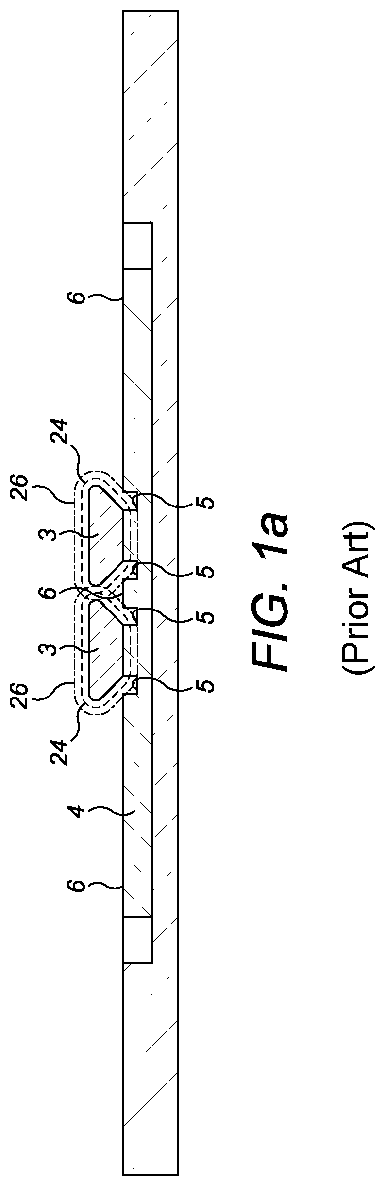
Electrode arrangement
a technology of electrodes and dielectric materials, applied in the field of electrodes, can solve the problem of nearly limited coupling of dielectric materials
- Summary
- Abstract
- Description
- Claims
- Application Information
AI Technical Summary
Benefits of technology
Problems solved by technology
Method used
Image

Examples
Embodiment Construction
[0060]In this specification, the term RF electrode refers to an electrode to which an RF voltage supply is connected. The term DC electrode herein refers to an electrode to which a DC voltage supply is connected. The term “inner” in relation to a surface herein refers to the surface that is facing towards the centre of the electrode assembly 100. The term “outer” in relation to a surface herein refers to the surface that is facing away from the centre of the electrode assembly 100.
[0061]FIG. 5 is a schematic diagram of a perspective view of an electrode assembly 100 in accordance with the present invention. The longitudinal axis of the electrode assembly 100 defines the longitudinal direction. The electrode assembly 100 extends in the longitudinal direction from a first end 100a to a second end 100b. The first and second ends 100a, 100b of the electrode assembly 100 are open / exposed for transport of ions therethrough.
[0062]The electrode assembly 100 has first and second electrode ar...
PUM
| Property | Measurement | Unit |
|---|---|---|
| RF voltages | aaaaa | aaaaa |
| RF voltages | aaaaa | aaaaa |
| resistance | aaaaa | aaaaa |
Abstract
Description
Claims
Application Information