

Etching mask, process for forming contact holes using same, and semiconductor device made by the process
- Summary
- Abstract
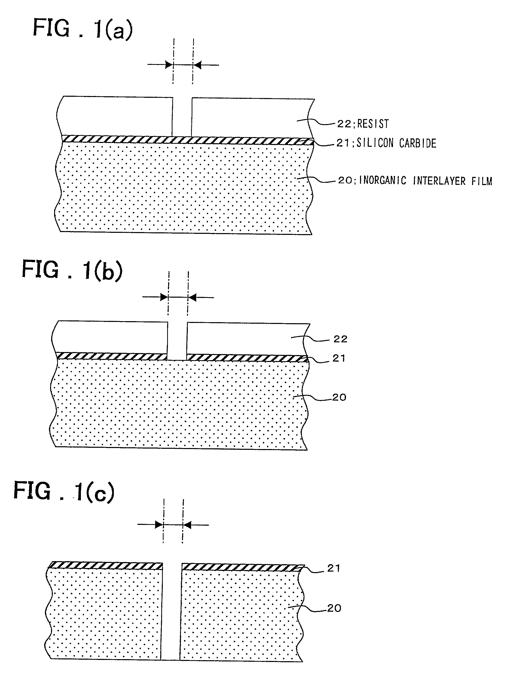
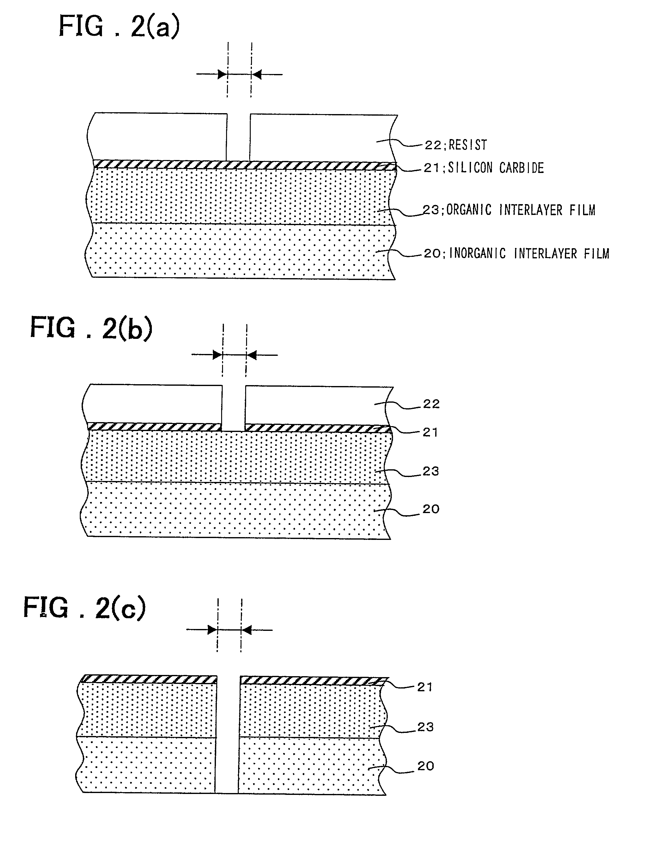
- Description
- Claims
- Application Information
AI Technical Summary
Benefits of technology
Problems solved by technology
Method used
Image

Examples
embodiment 1
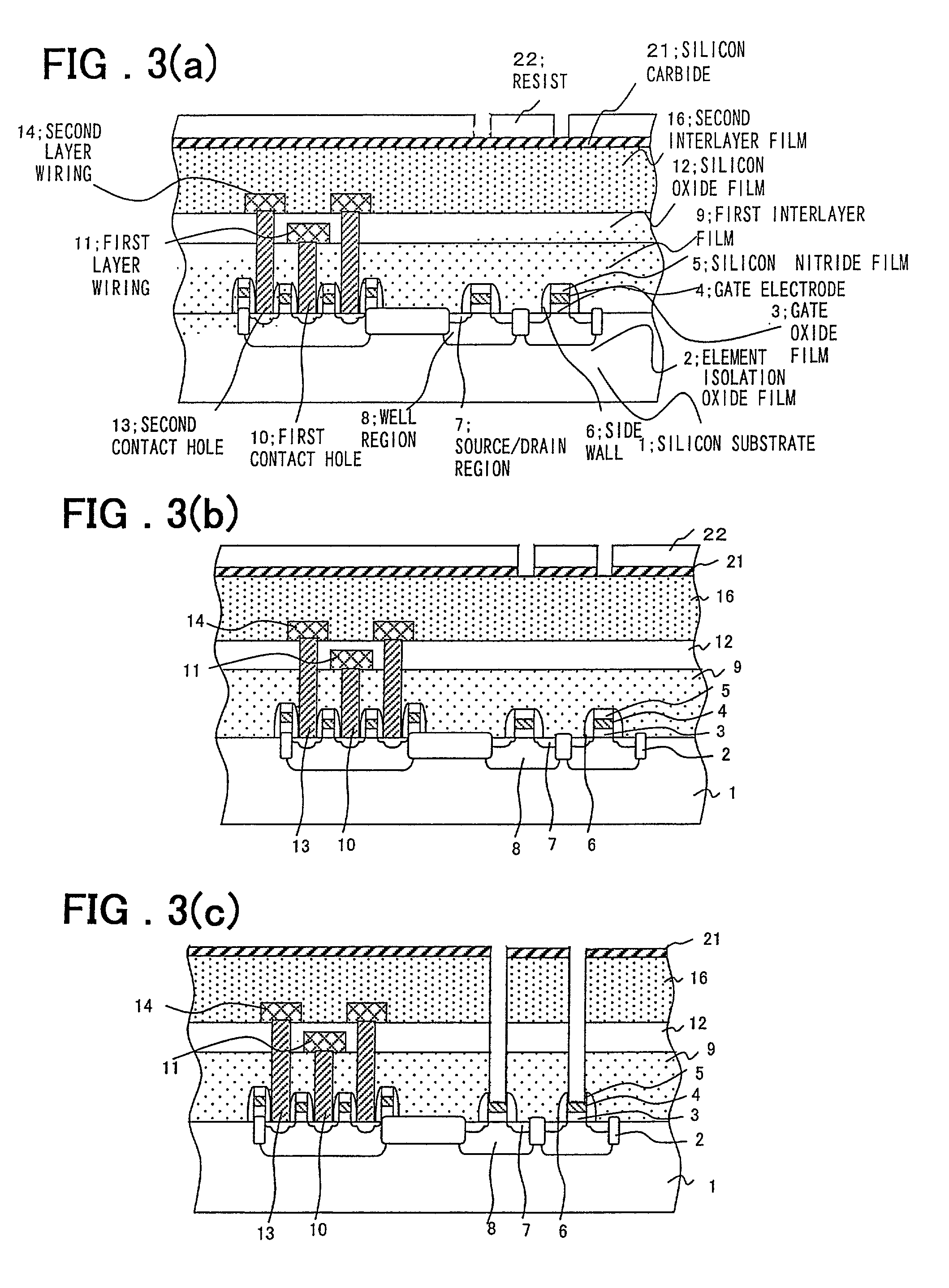
[0079] A DRAM of a first embodiment of the invention and a process for manufacturing the same will be described with reference to FIGS. 5 through 8. FIGS. 5 to 7 are sectional views schematically showing a process for manufacturing the DRAM of the first embodiment of the invention and are separated for convenience of drawing. FIG. 8 is a sectional view showing the structure of DRAM in case where the etching mask is not removed.
[0080] After an element isolation oxide film 2 is formed in given regions of a silicon substrate 1 by a trench isolation method as shown in FIG. 5(a), memory regions and peripheral circuit regions are formed. Well-regions 8 are formed by implanting ions of phosphorous, boron, etc. into respective regions. A gate oxide film 3, gate electrode 4 and silicon nitride film 5 are successively deposited on the silicon substrate 1 and gate electrodes are formed by etching process, followed by forming source / drain regions 7 by the implantation of ions of phosphorus and ...
PUM
 Abstract
Description
Claims
Application Information