
Plasma processes for depositing low dielectric constant films
a dielectric constant film and plasma technology, applied in the field of process and apparatus for depositing dielectric layers on a substrate, can solve the problems of affecting the overall performance of the device, and insufficient material as an etch stop layer
Patent Information
- Authority / Receiving Office
- US · United States
- Patent Type
- Applications(United States)
- Current Assignee / Owner
- Publication Date
- 2001-06-28
- Estimated Expiration
- Not applicable · inactive patent
Smart Images
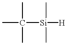
Figure 1 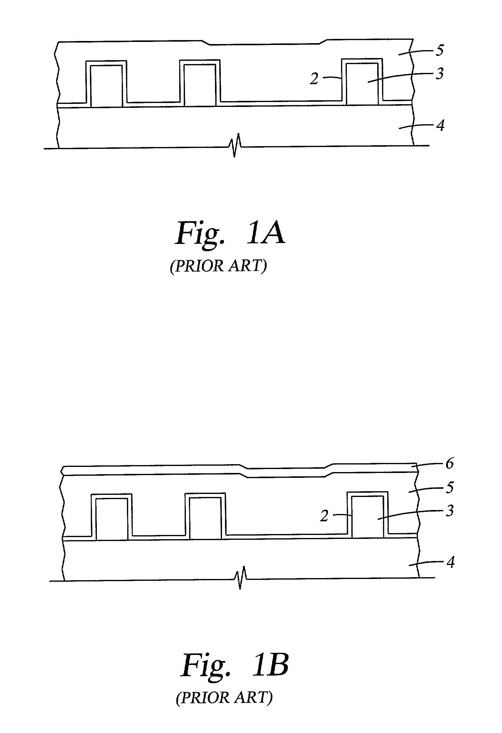
Figure 2 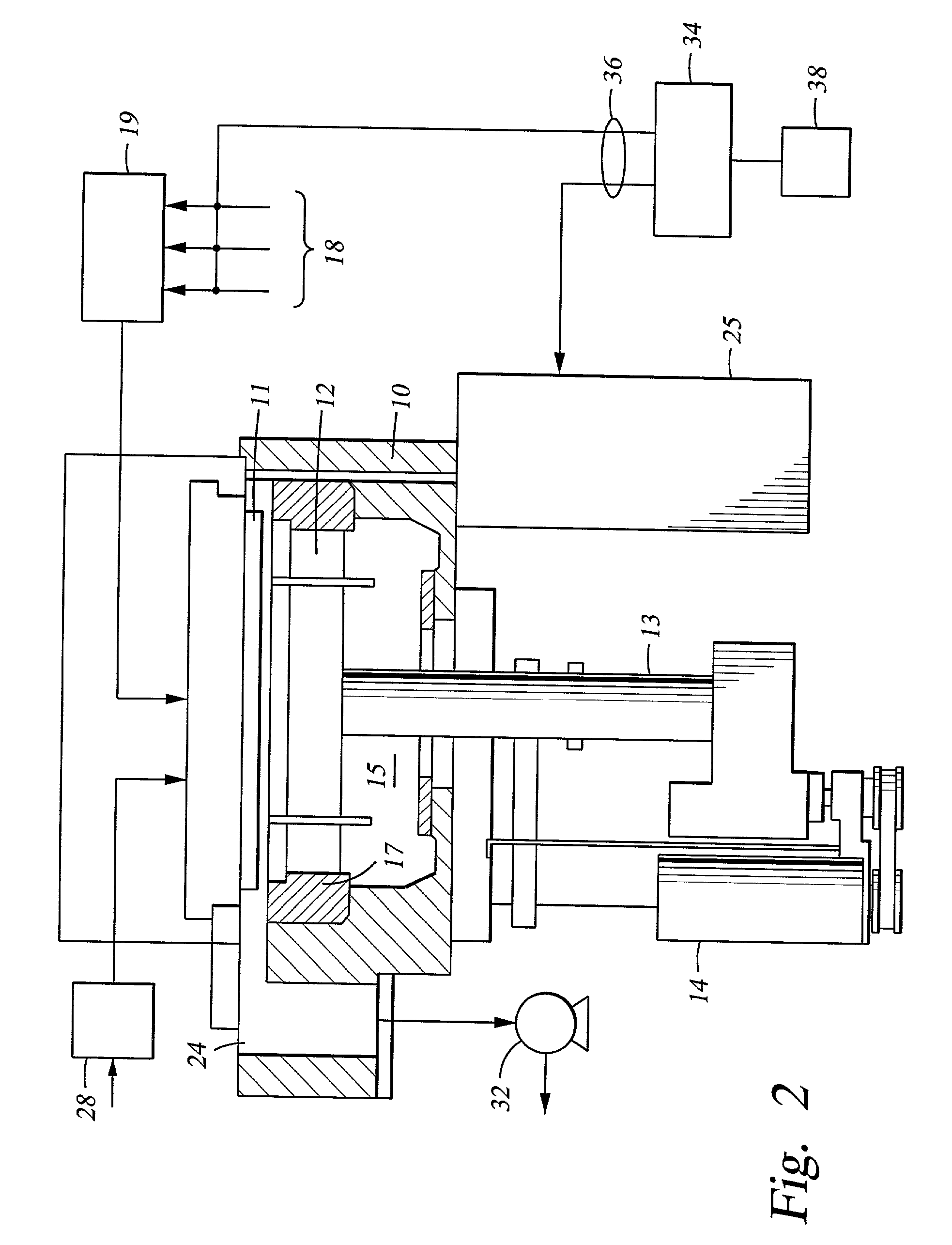
Figure 3
Abstract
Description
[0001] This application is a continuation-in-part of co-pending U.S. patent application Ser. No. 09 / 021,788, which was filed on Feb. 11, 1998, a continuation in part of co-pending U.S. patent application Ser. No. 09 / 114,682, which was filed on Jul. 13, 1998, a continuation-in-part of co-pending U.S. patent application Ser. No. 09 / 162,915, which was filed on Sep. 29, 1998; and a continuation-in-part of co-pending U.S. patent application Ser. No. 09 / 189,555, which was filed on Nov. 4, 1998.BACKGROUND OF THE DISCLOSURE
[0002] 1. Field of the Invention
[0003] The present invention relates to the fabrication of integrated circuits. More particularly, the invention relates to a process and apparatus for depositing dielectric layers on a substrate.
[0004] 2. Background of the Invention
[0005] One of the primary steps in the fabrication of modem semiconductor devices is the formation of metal and dielectric films on a substrate by chemical reaction of gases. Such deposition processes are referr...
Examples
example
[0106] The following example and demonstrates deposition of an oxidized organosilane or organosiloxane film having excellent barrier and adhesion properties. This example was undertaken using a chemical vapor deposition chamber, and in particular, a "CENTURA DxZ" system which includes a solid-state RF matching unit with a two-piece quartz process kit, both fabricated and sold by Applied Materials, Inc., Santa Clara, Calif.
Non-Pulsed RF Power
[0107] An oxidized dimethylsilane film was deposited at a chamber pressure of 3.0 Torr and temperature of 15EC from reactive gases which were flowed into the reactor as follows:
4 Dimethylsilane, (CH.sub.3).sub.2SiH.sub.2, at 55 sccm Nitrous oxide, N.sub.2O, at 300 sccm Helium, He, at 4000 sccm.
[0108] The substrate was positioned 600 mil from the gas distribution showerhead and 20 W of high frequency power (13 MHz) was applied to the showerhead for plasma enhanced deposition of an oxidized dimethylsilane layer. The oxidized dimethylsilane material...