Method of fabricating a single crystal ingot and method of fabricating a silicon wafer

a single crystal ingot and silicon wafer technology, applied in the direction of polycrystalline material growth, crystal growth process, protective fluid, etc., can solve the problem of reducing oxygen deposit due to the decrease of oxygen, increasing the width of the osf ring area, and unable to obtain predetermined gettering ability

Inactive Publication Date: 2001-10-18
COVALENT MATERIALS CORP
View PDF0 Cites 36 Cited by
  • Summary
  • Abstract
  • Description
  • Claims
  • Application Information

AI Technical Summary

Problems solved by technology

On the one hand, the oxygen deposit in the silicon wafer produced from this silicon single crystal ingot is essential to the IG method, however, the oxygen deposit is decreased due to the decrease of the oxygen.
Accordingly, a method by which nitrogen is doped in the polycrystalline silicon fused liquid, and the deposit of oxygen is promoted in the crystal of the silicon wafer, is conducted, however, the nitrogen doping generates a ring-like oxide induction lamination layer defect called OSF ring, when the thus produced silicon wafer is subjected to the thermal oxidization processing, and the width of the OSF ring area is increased.
Further, inside the OSF ring, the area in which the density of the oxygen deposit is greatly low exists, and in a portion in which the density of the oxygen deposit is greatly low and uneven, the gettering ability is lower than the other portion, and the predetermined gettering ability can not be obtained, and the oxide film with stand voltage is lowered, and the yield of the semiconductor device is lowered.
However, in this single crystal pulling up method, the productivity is lowered and the practicability is poor.
Further, in JP-A-11-195565, a method to produce the silicon wafer in which nitrogen is doped in the polycrystalline silicon; the single crystal is pulled up at low speed by using the Czochralski method; the nitrogen density is controlled; and the OSF ring is generated in the inside from the outer periphery of the crystal, or vanished at the central portion, is disclosed, however, the method is a method in which the single crystal is pulled up at the low speed, and the productivity is low and the practicability is poor.
Further, only by the size reduction of the COP by the increase of the pulling up speed (higher than 0.6 mm / min) disclosed in the official specification, the vanishing of the surface layer COP can not also be attained.
However, there is no consideration about which shape silicon single crystal is preferable.
Further, as the result of the advance of the temperature lowering of the process of the semiconductor device, the COP of 0.1-0.2 .mu.m level is hardly vanished in the process, and deteriorates the oxide film withstand voltage or the aging dielectric breakdown characteristic of the oxide film of the silicon wafer.

Method used


Image

  • Method of fabricating a single crystal ingot and method of fabricating a silicon wafer
  • Method of fabricating a single crystal ingot and method of fabricating a silicon wafer
  • Method of fabricating a single crystal ingot and method of fabricating a silicon wafer

Examples


third embodiment

[0093] According to the attached drawings, the method of fabricating the silicon wafer according to the present invention will be described below.

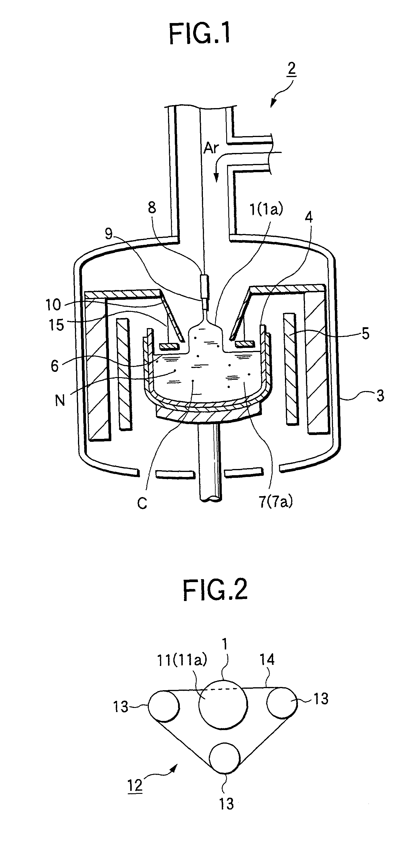
[0094] The silicon single crystal ingot used for the production a of the silicon wafer according to the present invention is pulled up by using the single crystal pulling up apparatus 1 as shown in FIG. 9.

[0095] For example, it is conducted in such a manner that polycrystalline silicon as a raw material is filled in the quartz glass crucible 4 arranged in the chamber 3 of the single crystal pulling up apparatus 2, further, as a dopant to dope nitrogen, a predetermined amount of silicon nitride is supplied in it, and the polycrystalline silicon is heated and fused by the heater 5 provided in the outer periphery of the quartz glass crucible 4, then, the seed crystal 9 attached onto the seed chuck 8 is dipped in the silicon fused liquid 7 into which nitrogen is doped, and while the seed chuck 8 and the quartz glass crucible 4 are rotated at a...

fourth embodiment

[0104] Next, the method of fabricating the silicon wafer according to the present invention will be described.

[0105] The present fourth embodiment is a method of fabricating the silicon wafer in which, after the silicon wafer produced in the same manner as the third embodiment, is specular-polished, by the hydrogen annealing, the density of the LSTD not below the dimension of 70 nm is made not lower than 3 pieces / cm.sup.2 in the area up to the depth of 5 .mu.m from the surface layer of the silicon wafer, and the BMD not below the dimension of 70 nm is made to exist with the high density in the area not below 10 .mu.m.

[0106] For example, in the same manner as in the third embodiment, the ingot is pulled up from the silicon fused liquid into which a predetermined amount of nitrogen is doped, and sliced, and the silicon wafer is produced. After this silicon wafer is specular-polished, it is hydrogen-annealed at the predetermined temperature, for a predetermined time period. By the hydr...

first embodiment

[0109] For example, in the same manner as in the first embodiment, it is conducted in such manner that the seed crystal 9 attached to the seed chuck is dipped in the silicon fused liquid into which a predetermined amount of the nitrogen is doped, and while the seed chuck and the quartz glass crucible are rotated at a predetermined rotating speed in the same direction or the reversal direction, the seed chuck is pulled up and the silicon single crystal ingot is grown, and it is pulled up at a predetermined pull-up speed. The nitrogen density of thus pulled up silicon single crystal ingot is made 6.times.10.sup.13-2.times.10.sup.15 atoms / cm.sup.3, and oxygen density is 0.8.times.10.sup.18-1.2.times.10.su-p.18 atoms / cm.sup.3. By the nitrogen doping, flocculation of the atomic holes in the silicon is suppressed, and the maximum size of the crystal defect is reduced.

[0110] When the nitrogen density is not larger than 6.times.10.sup.13 atoms / cm.sup.3, the growth of the crystal defect intr...


PUM

PropertyMeasurementUnit
sizeaaaaaaaaaa
sizeaaaaaaaaaa
temperatureaaaaaaaaaa

Abstract

A method of fabricating a silicon single crystal ingot and a method of fabricating a silicon wafer using the ingot, characterized in that: the method is structured in such a manner that the silicon single crystal ingot is pulled up from the silicon fused liquid 7 in which nitrogen N and carbon C are doped in polycrystalline silicon, by using the Czochralski method, and its nitrogen density is 1x10¹³-5x10¹⁵ atoms / cm3, and the carbon density is 5x10¹⁵-3x10¹⁶ atoms / cm3.

Description

BACKGROUND TECHNIQUE[0001] 1. Technical Field to which the Invention Belongs[0002] The present invention relates to method of fabricating a silicon single crystal ingot and method of fabricating a silicon wafer, and particularly to a method of fabricating the silicon single crystal ingot by which a yield of a semiconductor device can be increased. Further, particularly the present invention relates to a method of fabricating the silicon wafer by which a crystal defect of a surface layer is decreased, and the BMD density inside the wafer is increased.[0003] 2. Description of the Related Art[0004] The silicon wafer used for the semiconductor device is produced in such a manner that the single crystal ingot pulled up from a polycrystalline silicon by the CZ method is sliced.[0005] The CZ method is a method by which polycrystalline silicon as a raw material supplied into a quartz crucible is heated and fused, and a tip of a seed crystal is brought into contact with the silicon fused liq...

Claims


Application Information

Patent Timeline
Patent Type & Authority Applications(United States)
IPC IPC(8): C30B15/00C30B15/04
CPCC30B15/04C30B29/06
Inventor MINAMI, TOSHIROUHIRANO, YUMIKOIKEUCHI, KOUKIMIYAHARA, TAKASHIISHIKAWA, TAKASHIKUBOTA, OSAMUKOBAYASHI, AKIHIKO
Owner COVALENT MATERIALS CORP
Why Eureka
Try Eureka