
Touch panel substrate having transparent conductive film

a technology of conductive film and touch panel, which is applied in the direction of conductive layers on insulating supports, instruments, optical elements, etc., can solve the problems of difficult to stably obtain a given transmittance, difficulty in obtaining reproducible resistance values, and unsuitable film for use as electrodes in transparent touch panels

Inactive Publication Date: 2001-11-15
NIPPON SHEET GLASS CO LTD
View PDF0 Cites 37 Cited by
  • Summary
  • Abstract
  • Description
  • Claims
  • Application Information

AI Technical Summary

Benefits of technology

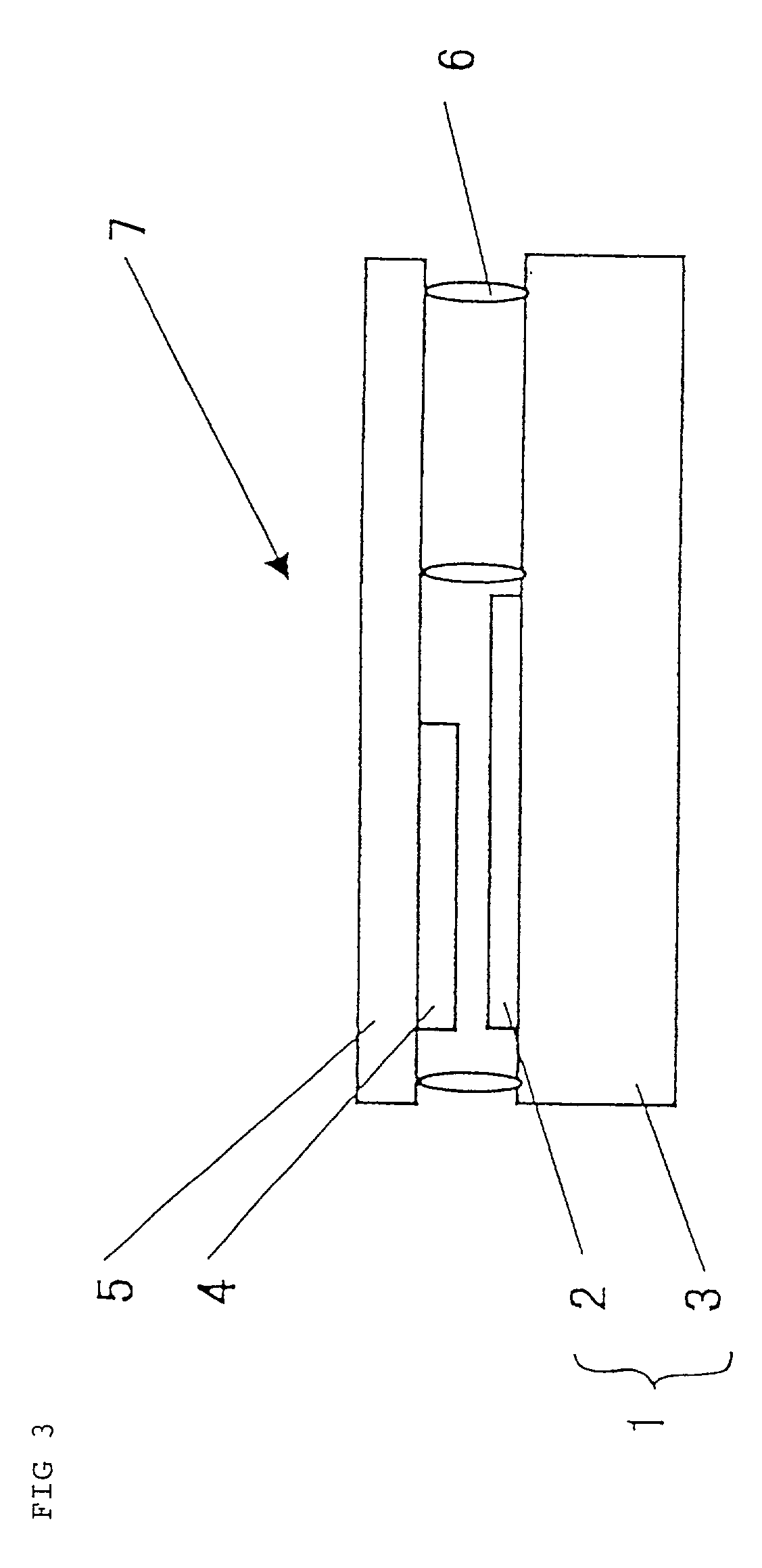
[0027] The invention further provides a resistive film type transparent touch panel employing the glass-based transparent touch panel substrate described above. This resistive film type transparent touch panel has satisfactory display quality because the transparent electrode has a high transmittance. Furthermore, by regulating the area of the transparent electrode to a given value, the touch panel can be of the power-saving type and switching operations can be conducted without fail.

Problems solved by technology

Because of this, the conventional transparent conductive film has a problem that the resistance thereof is so low as will be described later that the film is unsuitable for use as electrodes in transparent touch panels, in which the electrodes are required to have moderate sheet resistance.
There has been a problem that such reduced thicknesses result in difficulties in obtaining values of resistance with satisfactory reproducibility because of fluctuations of film deposition conditions, differences of heat history in a production process, etc.
Consequently, the substrates having this type of transparent conductive film have problems that it is difficult to stably obtain a given transmittance and that there is a large difference in transmittance between the uncoated areas of the transparent substrate and those areas of the transparent substrate which are coated with the transparent conductive film.
Due to this difference in transmittance, products employing this conventional substrate have a drawback that the areas coated with the transparent electrode are easily recognized.
However, the ITO film having such optical thickness equal to the half-wave length and hence attaining a high transmittance has a reduced value of resistance because of the inadequate specific resistance of the film.
Consequently, the transparent touch panel produced with this technique has a problem that the amount of current flowing through the panel in its ON state is large, resulting in increased power consumption.
However, there has been a problem that it is extremely difficult to process a tin oxide film in electrode formation therefrom and, in particular, it is difficult to use the tin oxide film to produce a touch panel having the function of delicate touch switching.
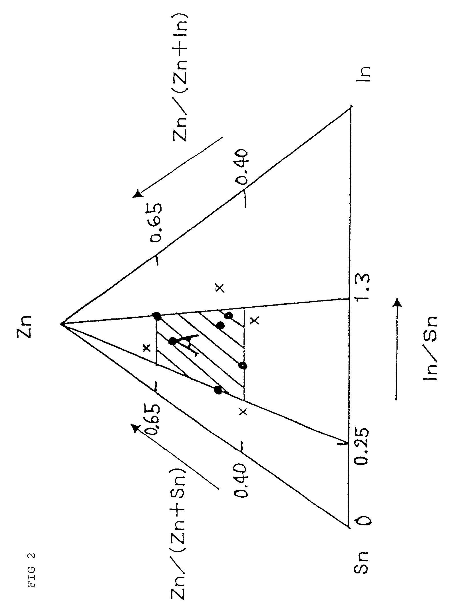
Zinc contents exceeding 65 atomic % are undesirable in that the film has too high a specific resistance and that the alkali resistance of the film abruptly becomes poor with increasing zinc content.
Furthermore, the metal oxide film having such too high a zinc content is undesirable in that the film, upon heating, e.g., in the step of laminating with a resin film, comes to have considerably increased electrical resistance and impaired heat resistance.
On the other hand, zinc contents lower than 40 atomic % based on all metals are undesirable in that the film has too low a specific resistance.
Indium atom contents in the film exceeding 1.3 times the content of tin atoms are undesirable in that the film has not only a reduced specific resistance but reduced wearing resistance.
Such too high indium contents are undesirable also from the standpoint of profitability because the cost of raw materials for the coating film is high.
Furthermore, such too high indium contents are apt to result in difficulties in stably depositing a film having a given resistance on a substrate by sputtering.
On the other hand, indium atom contents in the film lower than 0.25 times the content of tin atoms are undesirable in that the film has reduced solubility in acids and this makes it impossible to complete processing for electrode formation in a short time.
According to the embodiment described above, the transparent conductive film can be regulated so as to have a sheet resistance of about from 500 to 5,000 .OMEGA.. Sheet resistances of the transparent conductive film lower than 500 .OMEGA. are undesirable in that when two-transparent substrates each coated with the transparent conductive film are disposed so that the conductive films face each other to fabricate a touch panel, then the amount of current flowing upon contact of the opposed transparent conductive films (in the ON state) is large, resulting in increased power consumption.
On the other hand, sheet resistances of the transparent conductive film exceeding 5,000 .OMEGA. are undesirable in that the contact of the opposed conductive films results in unstable electrical connection.

Method used


Image

  • Touch panel substrate having transparent conductive film
  • Touch panel substrate having transparent conductive film
  • Touch panel substrate having transparent conductive film

Examples


examples 2 to 6

[0070] A transparent conductive film was deposited on a glass plate in the same manner as in Example 1, except that the target composition was changed. As shown in Table 1, the samples thus obtained each had a moderate sheet resistance in the range of from 500 to 5,000 .OMEGA. and a transmittance of 90% or higher. The samples obtained in Examples 1 to 6 each combined a high transmittance, moderate sheet resistance, and satisfactory processability in electrode formation and was an especially preferred sample of the substrate according to the invention. These samples were rated as .circleincircle. in comprehensive evaluation.

examples 7 to 10

[0071] A transparent conductive film was deposited on a glass plate in the same manner as in Example 1, except that the target composition was changed. As shown in Table 1, the samples thus obtained each had a transmittance of 91%. However, the sheet resistances of the samples obtained in Examples 7, 9, and 10 were 320 .OMEGA., 220 .OMEGA., and 390 .OMEGA., respectively, which were slightly lower than the lower limit in the moderate-resistance range shown above. These films were found to be effective in conducting ON / OFF operations without fail although less effective in power saving. On the other hand, the sample obtained in Example 8 had a transmittance of 92%, which was not lower than the transmittance of the glass plate, and had a sheet resistance of 9,800 .OMEGA., which was slightly higher than the upper limit in the desirable moderate-resistance range shown above. However, this sample was able to secure electrical connection upon contact of the transparent electrode in practic...


PUM

PropertyMeasurementUnit
Thicknessaaaaaaaaaa
Percent by atomaaaaaaaaaa
Fractionaaaaaaaaaa

Abstract

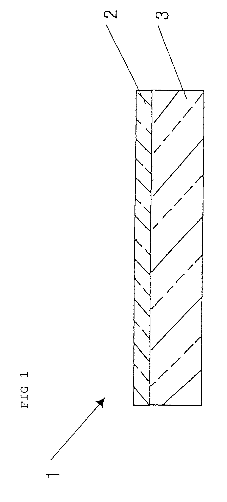
A transparent touch panel substrate comprising a transparent substrate and deposited thereon a transparent conductive metal oxide film which contains zinc, indium, and tin as metallic elements and is soluble in acids. The transparent conductive metal oxide film preferably contains zinc in an amount of from 40 to 65 atomic % based on all metals and contains indium in an amount of from 0.25 to 1.3 times the amount of tin on an atomic basis. The film preferably has a thickness of from 100 to 160 nm. Unlike the conventional substrate for resistive film type transparent touch panels which comprises a glass plate coated with a transparent conductive ITO film, the touch panel substrate of the invention combines three properties: high light transmittance; ease of processing in forming a transparent electrode by acid etching; and the transparent conductive film has a moderate sheet resistance of from 500 to 5,000 OMEGA. It therefore realizes a touch panel which combines the three functions of having satisfactory display quality, being of the power-saving type, and enabling touch switch operations to be conducted without fail.

Description

[0001] The present invention relates to a transparent touch panel substrate and a transparent touch panel employing the same.DESCRIPTION OF THE RELATED ART[0002] Indium oxide containing from 3 to 10% by weight tin oxide (hereinafter referred to as "ITO") for use as a transparent electrode in liquid-crystal displays is widely used as a transparent electrode formed on a transparent substrate for transparent touch panels, because it is transparent and can be easily processed in electrode formation. Transparent conductive tin oxide films also are used as transparent electrodes for transparent touch panels because they have satisfactory transparency.[0003] The composition of a transparent conductive ITO film for use in liquid-crystal displays is designed so that the film has the lowest possible value of electrical resistivity (specific resistance). Because of this, the conventional transparent conductive film has a problem that the resistance thereof is so low as will be described later ...

Claims


Application Information

Patent Timeline
IPC IPC(8): C23C14/08B32B17/10C23C14/34C23C14/35G06F3/041G06F3/045H01B5/14
CPCB32B17/10018B32B17/10174G06F3/045H01B5/14
Inventor TOYOSHIMA, TAKAYUKIARAI, DAISUKEANZAKI, TOSHIAKIOGINO, ETSUO
Owner NIPPON SHEET GLASS CO LTD
Learn More