Family of low power, regularly structured multipliers and matrix multipliers

a technology of regular structure and multipliers, applied in the field of family of low power, regularly structured multipliers and matrix multipliers, can solve the problems of significant load/wire imbalance, preventing significant advantages, and not addressing the issues of scalability, cost, power consumption and regularity,

Inactive Publication Date: 2001-12-27
THE RES FOUND OF STATE UNIV OF NEW YORK
View PDF12 Cites 13 Cited by
  • Summary
  • Abstract
  • Description
  • Claims
  • Application Information

AI Technical Summary

Problems solved by technology

These bounds vary from design to design, but generally prevent significant advantages from accruing to any one acceptable design.
Yu et al., in U.S. Pat. No. 5,790,446, apply matching-delay techniques and reduced interconnect lengths on a Booth-encoded or radix-4-encoded multiplier to improve speed and area usage, but such changes do not address issues of scalability, cost, power consumption and regularity.
In general, the traditional approaches to parallel multiplication have three major drawbacks in the design of high performance larger size (say 64.times.64-bit) multipliers: first, design irregularity is inherent in the bit reduction of a large partial product matrix (even using Booth recoding) into two numbers; second, significant load / wire imbalance arises due to the differing column heights of the large partial product network; third, these multipliers exhibit a large power dissipation due to the use of large number of high-speed, small-size binary logic parallel counters such as (3, 2) and (4, 2).
For larger multipliers, this approach is not effective.
Using software on a core central processor to perform matrix multiplication computation is wasteful of both time and hardware resources.
Hardware implementation of an expanded multiplier in a computer-arithmetic system improves multiplication performance in terms of speed, but inevitably faces limitations on the amount of VLSI area available.
Excessive VLSI area usage impacts both cost and performance.
Restricting VLSI area in the design of such a processor introduces a conflict between its versatility and computation speed.
Coupled with VLSI area restrictions, such a large multiplier circuit curtails the number of items which can be concurrently stored and processed in the matrices.
Consequently, multiplication of input matrices with a large number of lower precision items results in waste of the 64-bit hardware.
But if the hardware is designed to handle the low-precision cases by reducing the size of the multipliers to 8.times.8 bits or 16.times.16 bits, matrix multiplication for input arrays with higher precision items become impossible without the use of slow software methods.
All of the known architectures have two general drawbacks: First, they provide no solution to the above design conflict problems; all multipliers used in those systems have a fixed size.
This makes them inefficient in handling inputs with a precision lower than the fixed size, and incapable of processing inputs with higher precision.
Second, they display large power dissipation, which is a major concern in VLSI design.

Method used


Image

  • Family of low power, regularly structured multipliers and matrix multipliers
  • Family of low power, regularly structured multipliers and matrix multipliers
  • Family of low power, regularly structured multipliers and matrix multipliers

Examples


Embodiment Construction

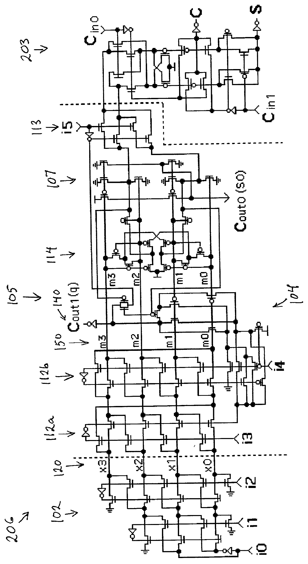
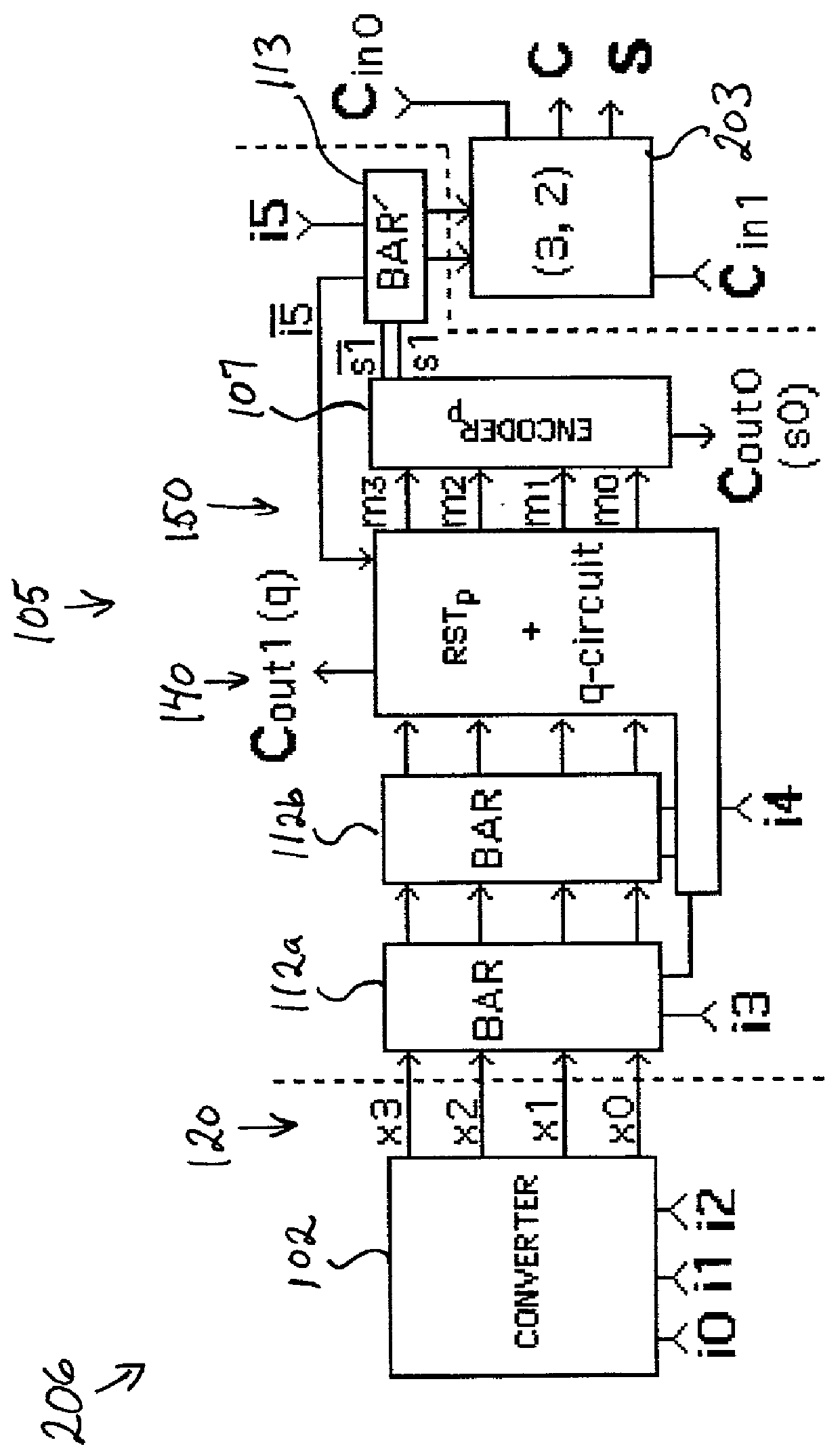
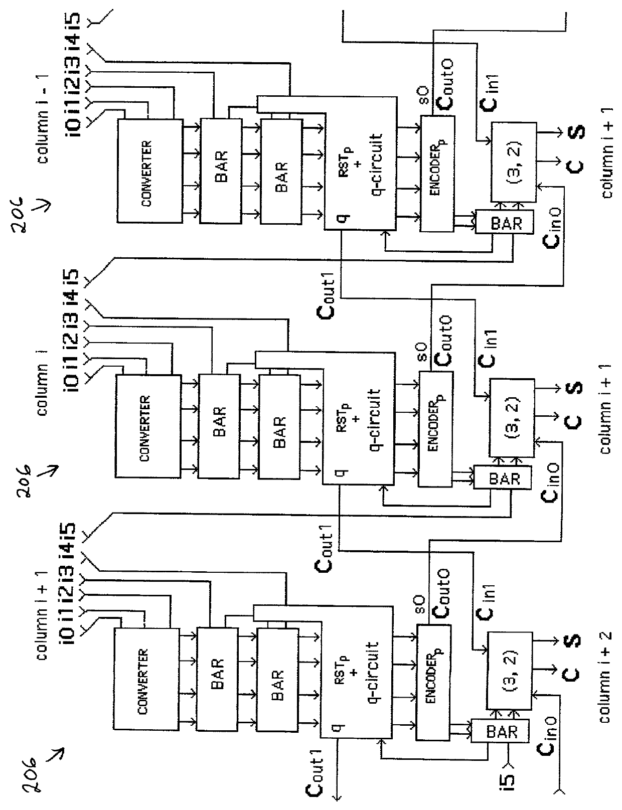
[0139] The present invention comprises numerous multiplier embodiments constructed using three essential major features: a partial product matrix reduction circuit using (6, 2) based parallel counters, a regularly-structured multiplier, and a reconfigurable multiplier. All three features derive unique value from the innovative shift switch circuits and methods which are the subject of U.S. Pat. No. 6,125,379, incorporated herein by reference.

[0140] The first major feature of the present invention is the shift-switch-based partial product matrix reduction circuit, which supports rapid and compact multiplication of two 64-bit numbers or two 64-bit floating point numbers with 53-bit mantissas. The second feature of the invention incorporates the first feature in a regularly structured design which applies a novel square recursive decomposition to the partial product matrix to produce a fast, simply-interconnected, and trace-optimized multiplier architecture. The third feature of the in...


PUM


Abstract

A family of embodiments of a new class of CMOS VLSI computer multiplier circuits that are simpler to fabricate, smaller, faster, more efficient in their use of power, and easier to scale in size than the prior art. The normal binary adder circuit unit is replaced by the innovative shift switch circuit unit. Use of the shift switch circuit sharply reduces fluctuations of power caused by plurality variations in the bit representations of the input, intermediate and output numbers. Reduced-scale devices are used in shift-switch pass-transistor signal restoration circuits, significantly reducing the size, power demand, and power dissipation of internal circuitry, in contrast to ordinary multiplier design. The simplicity of the circuit design allows multiplier partial-product reduction in fewer logic stages than existing comparable designs allow, showing speed improvement over such designs. The circuit design simplicity and the use of reduced-scale devices require less VLSI area than existing designs need, facilitating integration in VLSI microprocessors. Modular circuit organization simplifies scaling for larger operands without the circuit complications of existing designs. The design includes a critical flip of the physical layout of the partial-product matrix at each size level, simplifying the layout of traces in the circuit at all size scales. Finally, the application of reconfigurable design principles to the easily-scaled layout reduces significantly the mean demand for computing resources over a wide range of multiplication bit-width scales, as compared to existing designs. Overall, the orchestrated integration of these diverse design innovations makes possible the implementation of simpler, faster, smaller, more efficient, more flexible, and easier-to-build VLSI multiplication circuits than the current art reveals.

Description

This patent claims the benefit of the priority date of U.S. Pat. No. 6,125,379 filed Feb. 11, 1998 and Ser. No. 60 / 190,438 filed Mar. 17, 2000 and Ser. No. 09 / 415,380 filed Feb. 21, 2000.[0001] The present invention relates generally to very-large-scale integrated (VLSI) circuits, and more specifically to low-power, high-performance VLSI multiplier circuits.DEFINITIONS[0002] The term "p-type 4-bit state signal" here refers to a column of four bits, where only one bit is 1 and the other three bits are all 0. The value of the state signal is I (0.ltoreq.I.ltoreq.3) if the 1 bit is in position I.[0003] The term "n-type 4-bit state signal" here refers to an signal with an opposite representation to a p-type state signal, i.e. the unique bit is 0, instead of 1.[0004] The term "binary-to-state signal converter" here refers to a circuit which produces a shift switch signal representing a count of the number of independent input signal lines in an "on" state. Each distinct shift switch sign...

Claims


Application Information

Patent Timeline
Patent Type & Authority Applications(United States)
IPC IPC(8): G06F7/50G06F7/52G06F7/60
CPCG06F7/501G06F7/5318G06F7/5324G06F7/60G06F7/607G06F2207/382G06F2207/3828
Inventor LIN, RONG
Owner THE RES FOUND OF STATE UNIV OF NEW YORK
Why Eureka
Try Eureka